
System and method for generating a clock gating network for logic circuits

a logic circuit and clock gating technology, applied in pulse generators, power consumption reduction, pulse techniques, etc., can solve the problem of significant reduction of the total clock tree switching power, and achieve the effect of reducing switching power consumption and enabling the quantification of expected power savings

Inactive Publication Date: 2013-08-01
BAR ILAN UNIV
View PDF6 Cites 25 Cited by
  • Summary
  • Abstract
  • Description
  • Claims
  • Application Information

AI Technical Summary

Benefits of technology

This patent text discusses a method for reducing power consumption in integrated circuits by using data transmission networks that are controlled by a clock signal. The text introduces a new model that can be used to estimate the expected power savings and the impact on performance. The text also presents several efficiency improvements that can be made to existing clock gating systems. Overall, the technical effect of this patent is to provide a more effective and efficient method for controlling clock signals in integrated circuits to reduce power consumption.

Problems solved by technology

The resulting clock gating methodology may significantly reduce the total clock tree switching power significantly.

Method used


Image

  • System and method for generating a clock gating network for logic circuits
  • System and method for generating a clock gating network for logic circuits
  • System and method for generating a clock gating network for logic circuits

Examples


Embodiment Construction

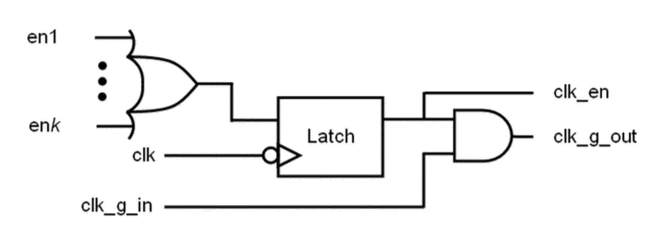
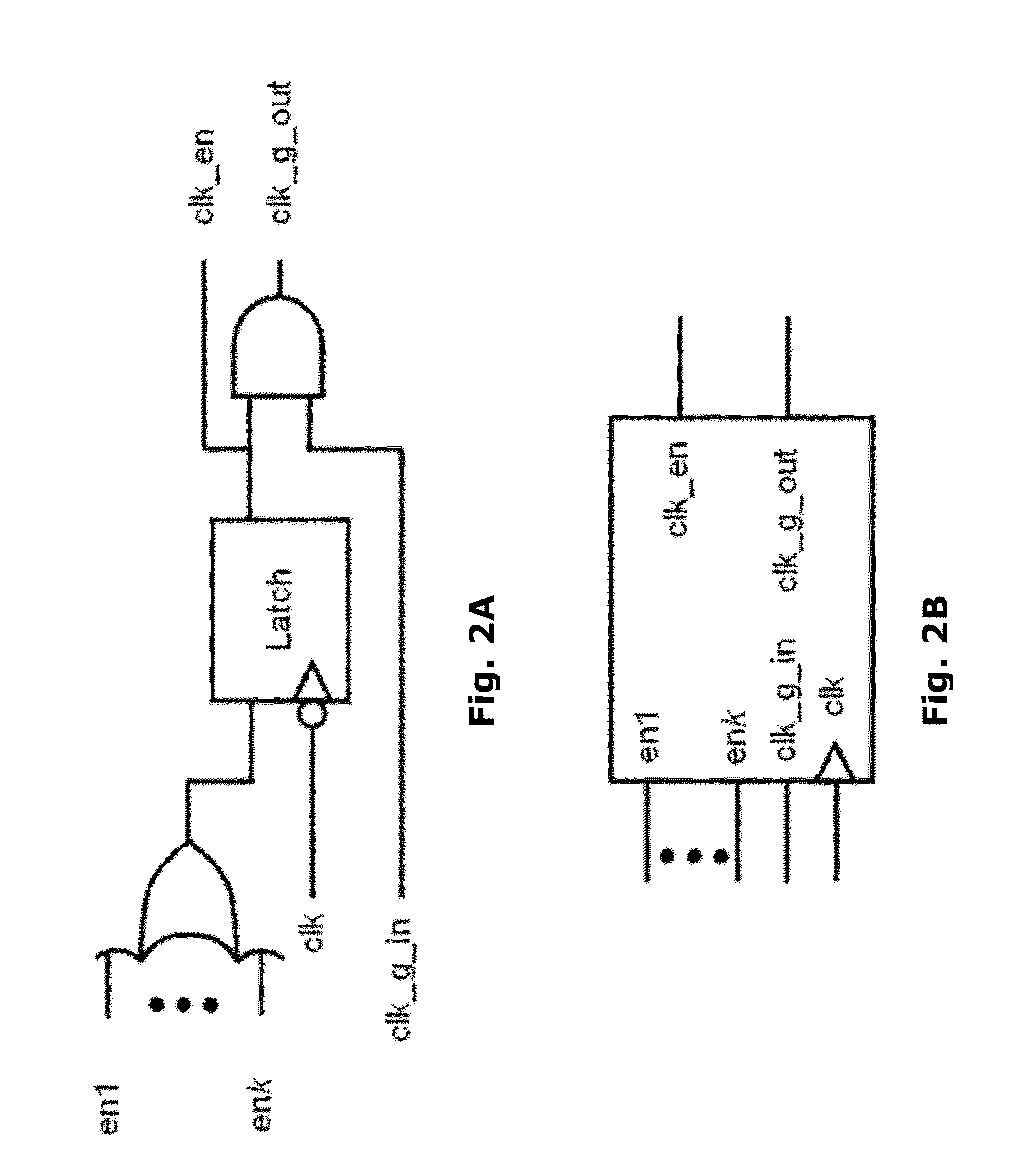
[0050]Aspects of the present disclosure relate to the gating of Very Large Scale Integration (VLSI) circuits. In particular embodiments are presented for the generation of gating networks based upon the actual behavior of a logic circuit or systems' component registers, such as flip-flops (FFs).

[0051]Optionally, statistical analysis of register behavior is performed on a simulation of a test bench of the logic circuit or system to determine the correlation between toggling behavior of the registers. Correlated registers may be clustered into sets and driven by a common clock gater. Such gated clusters may themselves be clustered into correlated sets and driven by higher level gaters as required. It is noted that number of levels of a gating network and the number of registers in each cluster may be determined from an analysis such as disclosed hereinbelow.

[0052]It is noted that the systems and methods of the disclosure herein may not be limited in its application to the details of c...


PUM


Abstract

A system and method for generating a power efficient clock gating network for a Very Large Scale Integration (VLSI) circuit. Statistical analysis is performed upon the activity of component registers of the circuit and registers having correlated toggling behavior are clustered into sets and provided with common clock gaters. The clock gating network may be generated independently from the logical structure of the circuit.

Description

FIELD AND BACKGROUND OF THE INVENTION[0001]The disclosure herein relates to Very Large Scale Integration (VLSI) circuit and system design. In particular the disclosure relates to statistically determined clock gating networks and their application to power efficient logic circuits and systems.[0002]The increasing demand for low power mobile computing and consumer electronics products has refocused Very Large Scale Integration (VLSI) design in the last two decades on lowering power and increasing energy efficiency. In particular, power reduction is treated at all design levels of VLSI chips, from architecture through block and logic levels, down to gate-level, circuit and physical implementation.[0003]One of the major dynamic power consumers is the system's clock signal, which may be responsible for up to 50% of the total dynamic power consumption or more. Clock network design is a delicate procedure, and may be therefore done in a very conservative manner under worst case assumption...

Claims


Application Information

Patent Timeline
IPC IPC(8): H03K3/00
CPCH03K19/0016
Inventor WIMER, SHMUEL
Owner BAR ILAN UNIV
Learn More