
Organic Spintronic Devices and Methods for Making the Same

a spintronic and organic technology, applied in thermoelectric devices, solid-state devices, nano-informatics, etc., can solve the problems of environmental damage and/or risk, none of these energy sources satisfactorily eliminate environmental concerns, widespread use, etc., to improve the efficiency of oled and charge mobility in fet devices, and increase the relaxation rate of spin lattices

Inactive Publication Date: 2013-08-08
UNIV OF UTAH RES FOUND
View PDF0 Cites 17 Cited by
  • Summary
  • Abstract
  • Description
  • Claims
  • Application Information

AI Technical Summary

Benefits of technology

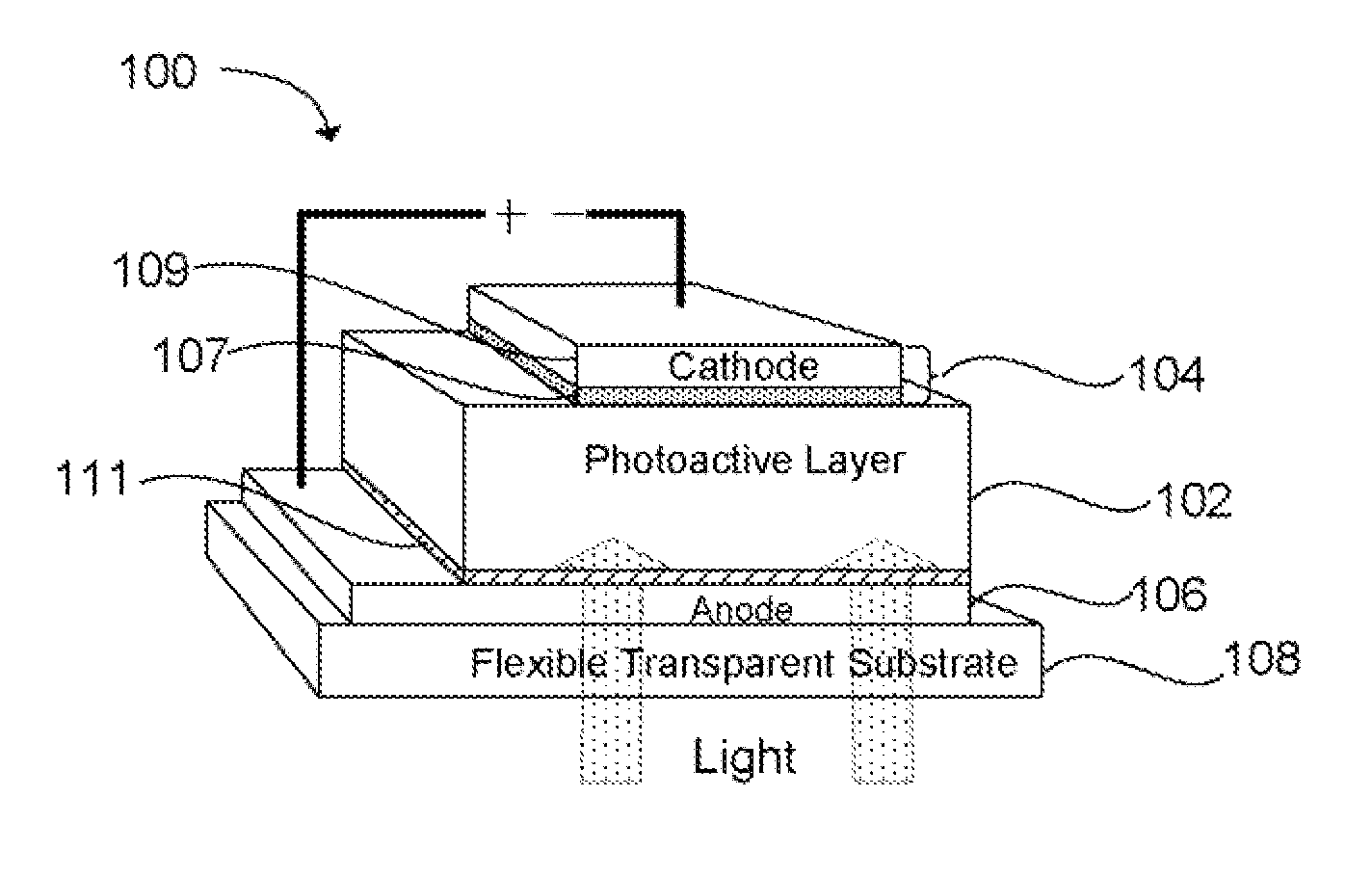
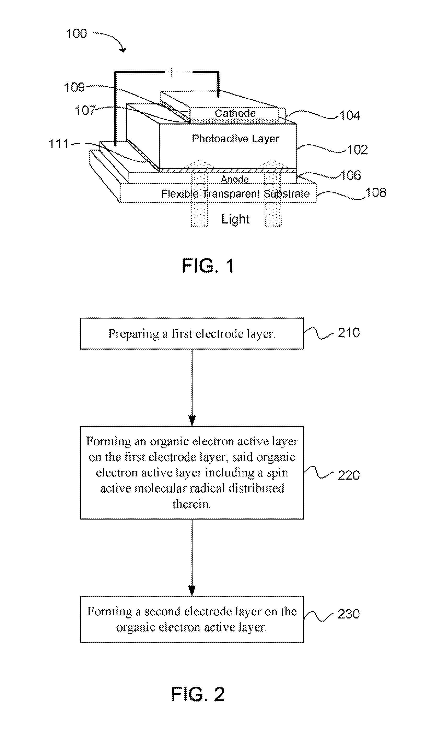
The patent text describes an organic spintronic photovoltaic device that uses an organic electron active layer with a spin active molecular radical to increase spin-lattice relaxation rates. The device can be designed in a variety of configurations and can also include other layers such as a donor material, acceptor material, and redox coupling electrolyte. The use of the spin active molecular radical can lead to increased efficiency and mobility in FET devices. The method of manufacturing the device involves preparing electrode layers and forming the organic electron active layer on top. Overall, the patent presents a new technology for organic photovoltaics that can enhance spin-lattice relaxation rates to improve performance.

Problems solved by technology

Conventional energy sources such as coal, oil, natural gas, and uranium, represent a finite resource and furthermore result in adverse consequences in terms of environmental damage and / or risk of damage.
Despite some improvements in pollution control and safety protocols, none of these energy sources satisfactorily eliminates environmental concerns.
Each of these technologies currently has economic, practical, and / or technical hurdles which prevent their widespread use.
The technology of photovoltaic devices is well developed, but large scale application is hampered by the high price of the cells.
The widespread use of solar power has been elusive because it can be difficult and costly to manufacture commercial photovoltaic cells, which are made of inorganic crystals such as silicon.
Unfortunately, poor energy conversion efficiencies have thus far prevented organic-based devices from being successfully commercialized.
However, none of the existing techniques provides sufficient improvements in efficiencies and reduced manufacturing costs.

Method used


Image

  • Organic Spintronic Devices and Methods for Making the Same
  • Organic Spintronic Devices and Methods for Making the Same
  • Organic Spintronic Devices and Methods for Making the Same

Examples


examples

[0067]Without being bound to any particular theory, one of the main contributing factors to the low efficiency appears to be the low output current due to the high carrier recombination rate and low carrier mobility. In bulk heterojunction organic photovoltaics, the accepted mechanism for current production is the following: First, upon illumination, there is exciton generation in the blend, followed by a migration of the exciton to the donor-acceptor interface where, either because of the existence of a build in potential or the dipole interaction between the donor and the acceptor, this exciton is separated into a free electron in the acceptor material and a hole in the donor material. From this point, the electron and hole migrate to the cathode and the anode, respectively. For efficient device performance, one has an exciton diffusion length that is larger than the average donor or acceptor aggregate size to minimize exciton recombination. For efficient exciton separation the ex...


PUM

PropertyMeasurementUnit
wt %aaaaaaaaaa
wt %aaaaaaaaaa
wavelengthaaaaaaaaaa

Abstract

An organic spintronic photovoltaic device (100) having an organic electron active layer (102) functionally associated with a pair of electrodes (104, 106). The organic electron active layer (102) can include a spin active molecular radical distributed in the active layer (102) which increases spin-lattice relaxation rates within the active layer (102). The increased spin lattice relaxation rate can also influence the efficiency of OLED and charge mobility in FET devices.

Description

RELATED APPLICATIONS[0001]Priority of U.S. Provisional Patent Application Ser. No. 61 / 103,817 filed on Oct. 8, 2008 is claimed.GOVERNMENT INTEREST[0002]This invention was made with government support under Department of Energy Grant No. 04-ER 46109 and National Science Foundation Grant Nos. 05-03172 and 08-03172. The United States government has certain rights in this invention.FIELD OF THE INVENTION[0003]This invention relates to electronic devices based on organic semiconducting materials. More specifically, the invention covers organic spintronic photovoltaic devices having unique organic compositional features. Therefore, the present invention relates generally to the fields of electrical engineering, quantum physics, chemistry, materials science, spintronics, and photovoltaic applications.BACKGROUND[0004]Conventional energy sources such as coal, oil, natural gas, and uranium, represent a finite resource and furthermore result in adverse consequences in terms of environmental da...

Claims


Application Information

Patent Timeline
Patent Type & Authority Applications(United States)
IPC IPC(8): H01L51/42H10K99/00
CPCB82Y10/00H01L51/442H01L51/0037H01L51/004H01L51/0047H01L51/005H01L51/4253Y02E10/549H01L51/424H01L51/0038H01L51/0035H01L51/0067H01L51/0059H01L51/0058H01L51/0036H10K85/113H10K85/1135H10K85/141H10K85/215H10K85/60H01G9/2004H10K30/30H10K30/20H10K30/82H10K85/111H10K85/114H10K85/626H10K85/631H10K85/654
Inventor VARDENY, ZEEVVALENTINENDOBE, ALEX
Owner UNIV OF UTAH RES FOUND
Learn More