Method for manufacturing semiconductor device

a semiconductor film and manufacturing method technology, applied in the direction of semiconductor devices, electrical devices, transistors, etc., can solve the problems of long deposition time, low throughput, and leakage current flow, and achieve efficient diffusion, reduce oxygen vacancies in the oxide semiconductor film, and diffuse

Inactive Publication Date: 2013-08-08
SEMICON ENERGY LAB CO LTD
View PDF2 Cites 115 Cited by
  • Summary
  • Abstract
  • Description
  • Claims
  • Application Information

AI Technical Summary

Benefits of technology

[0027]The oxide insulating film and the metal oxide film to which oxygen is added are used as a gate insulating film of a transistor including an oxide semiconductor film. That is, the oxide insulating film in contact with the oxide semiconductor film contains the oxygen. Further, the metal oxide film functions as an oxygen diffusion prevention film. Accordingly, oxygen in the oxide insulating film can be efficiently diffused into the oxide semiconductor film by heat treatment so that oxygen vacancies in the oxide semiconductor film can be reduced.
[0028]An oxide insulating film is formed over a top-gate transistor including an oxide semiconductor film and a metal film is formed over the oxide insulating film; after that, oxygen can be added to the metal film and added also to the oxide insulating film. That is, the oxide insulating film contains the oxygen. Further, the metal oxide film functions as an oxygen diffusion prevention film. Accordingly, the oxygen in the oxide insulating film can be...

Problems solved by technology

In the case where an aluminum oxide film is formed by an atomic layer deposition method, a forming process and an oxidization process of an aluminum layer with an atomic-layer-level thickness are alternately perfo...

Method used


Image

  • Method for manufacturing semiconductor device
  • Method for manufacturing semiconductor device
  • Method for manufacturing semiconductor device

Examples


embodiment 1

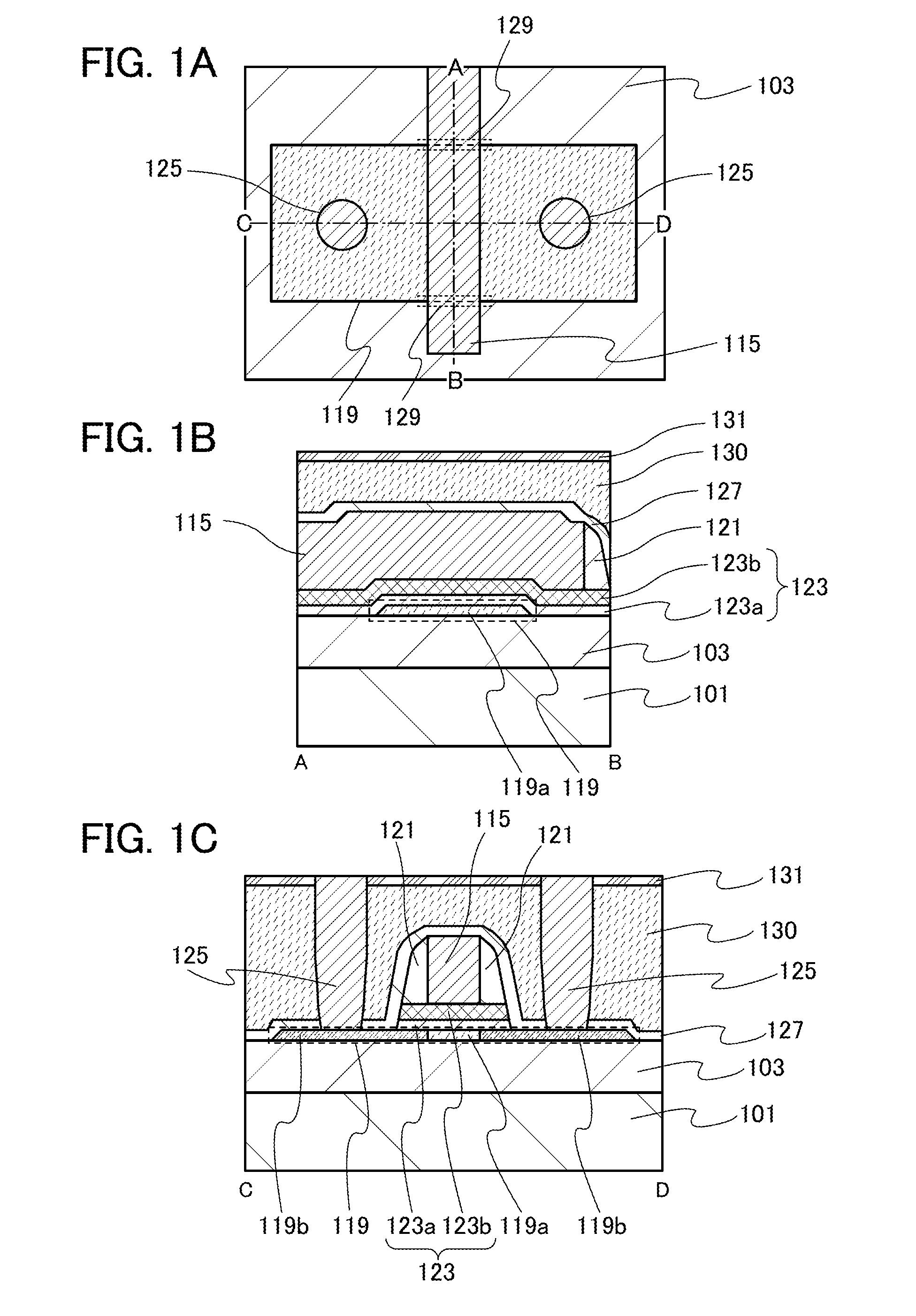
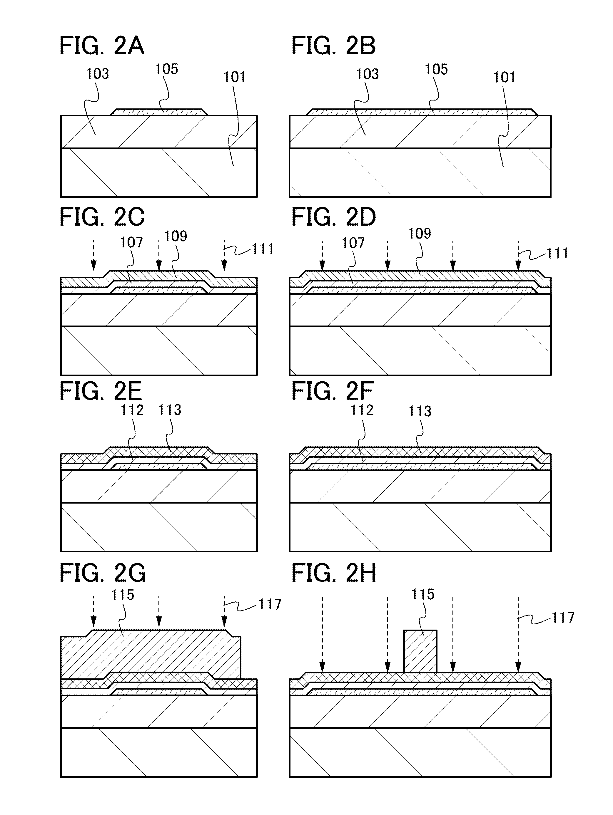
[0057]In this embodiment, a structure of a transistor having excellent electrical characteristics and a method for manufacturing the transistor with high productivity are described with reference to FIGS. 1A to 1C, FIGS. 2A to 2H, FIGS. 3A to 3F, and FIGS. 4A to 4H.

[0058]FIGS. 1A to 1C are a top view and cross-sectional views of a transistor described in this embodiment. FIG. 1A is a top view of the transistor described in this embodiment. FIG. 1B is a cross-sectional view in the channel width direction of the transistor taken along dashed-dotted line A-B in FIG. 1A. FIG. 1C is a cross-sectional view in the channel length direction of the transistor taken along dashed-dotted line C-D in FIG. 1A. Note that in FIG. 1A, illustration of some components of the transistor (e.g., a gate insulating film 123, sidewalls 121, an insulating film 127, and an interlayer insulating film 130) is omitted for clarity.

[0059]The transistor illustrated in FIGS. 1A to 1C includes an oxide insulating film...

embodiment 2

[0246]In this embodiment, a transistor in which a metal oxide film formed by oxidizing a metal film is used as a gate insulating film and a method for manufacturing the transistor are described with reference to FIGS. 1A to 1C, FIGS. 2A to 2H, FIGS. 3A to 3F, FIGS. 4A to 4H, and FIGS. 5A and 5B. The transistor in this embodiment is different from that in Embodiment 1 in that only the metal oxide film formed by adding oxygen to a metal film is the gate insulating film.

[0247]FIGS. 5A and 5B are cross-sectional views of the transistor described in this embodiment. The top view of the transistor illustrated in FIGS. 5A and 5B is similar to that in FIG. 1A described in Embodiment 1, and thus is not illustrated here. FIG. 5A is a cross-sectional view in the channel width direction of the transistor, which corresponds to the dashed-dotted line A-B in FIG. 1A. FIG. 5B is a cross-sectional view in the channel length direction of the transistor, which corresponds to the dashed-dotted line C-D...

embodiment 3

[0258]In this embodiment, a transistor in which a metal oxide film formed by oxidizing a metal film is used as a protective film for the transistor and a method for manufacturing the transistor are described with reference to FIGS. 1A to 1C, FIGS. 2A to 2H, and FIGS. 3A to 3D, and FIGS. 6A and 6B.

[0259]FIGS. 6A and 6B are cross-sectional views of the transistor described in this embodiment. The top view of the transistor illustrated in FIGS. 6A and 6B is similar to that in FIG. 1A described in Embodiment 1, and thus is not illustrated here. FIG. 6A is a cross-sectional view in the channel width direction of the transistor, which corresponds to the dashed-dotted line A-B in FIG. 1A. FIG. 6B is a cross-sectional view in the channel length direction of the transistor, which corresponds to the dashed-dotted line C-D in FIG. 1A.

[0260]The transistor illustrated in FIGS. 6A and 6B includes the oxide insulating film 103 over the substrate 101, the oxide semiconductor film 119 over the oxide...


PUM


Abstract

To improve productivity of a transistor that includes an oxide semiconductor and has good electrical characteristics. In a top-gate transistor including a gate insulating film and a gate electrode over an oxide semiconductor film, a metal film is formed over the oxide semiconductor film, oxygen is added to the metal film to form a metal oxide film, and the metal oxide film is used as a gate insulating film. After an oxide insulating film is formed over the oxide semiconductor film, a metal film may be formed over the oxide insulating film. Oxygen is added to the metal film to form a metal oxide film and added also to the oxide semiconductor film or the oxide insulating film.

Description

BACKGROUND OF THE INVENTION[0001]1. Field of the Invention[0002]The present invention relates to a method for manufacturing a semiconductor device.[0003]In this specification, a semiconductor device means all types of devices that can function by utilizing semiconductor characteristics, and an electro-optical device and a semiconductor integrated circuit are semiconductor devices.[0004]2. Description of the Related Art[0005]A transistor whose channel region includes a semiconductor thin film over an insulating surface is applied to a wide range of electronic devices such as an integrated circuit (IC) or an image display device (display device). A silicon-based semiconductor material is widely known as a material for a semiconductor thin film applicable to the transistor. In recent years, attention has been drawn to a technique by which a transistor whose channel region includes an oxide semiconductor instead of silicon to be applied to an electronic device or an optical device. For ...

Claims


Application Information

Patent Timeline
IPC IPC(8): H01L21/02
CPCH01L21/0237H01L21/441H01L29/517H01L29/41733H01L27/1225H01L29/7869H01L27/10873H01L27/1108H01L27/1156H01L29/66969H10B12/05H10B10/125H10B41/70H01L21/02244H01L21/02178H01L21/02565H01L21/383H01L21/425H01L21/47573H01L29/24H01L29/4908H01L29/495
Inventor ISOBE, ATSUOHOSOYA, KUNIO
Owner SEMICON ENERGY LAB CO LTD
Why Eureka
Try Eureka