Separation membrane, hydrogen separation membrane including the separation membrane, and hydrogen purifier including the hydrogen separation membrane
a technology of separation membrane and separation membrane, which is applied in the direction of membranes, other chemical processes, separation processes, etc., can solve the problem of high unit cost of pd-based metal and limit its commercialization
- Summary
- Abstract
- Description
- Claims
- Application Information
AI Technical Summary
Benefits of technology
Problems solved by technology
Method used
Image
Examples
example 1
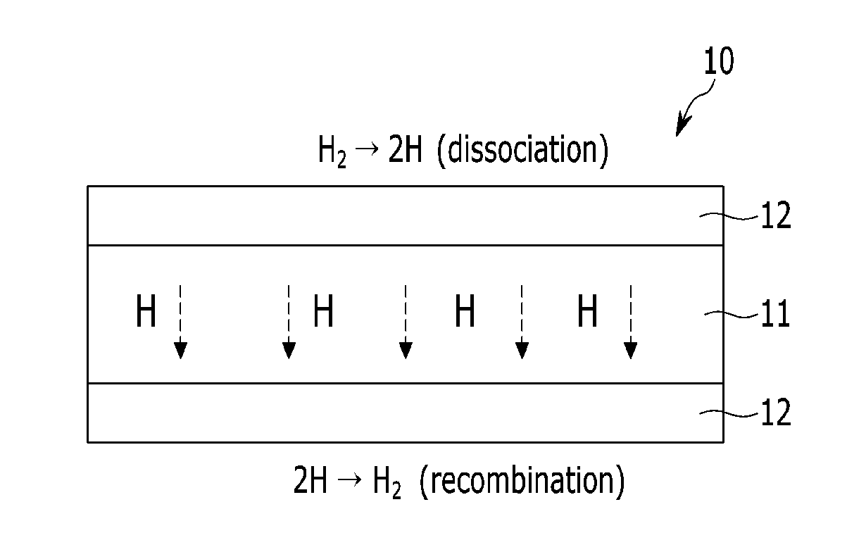
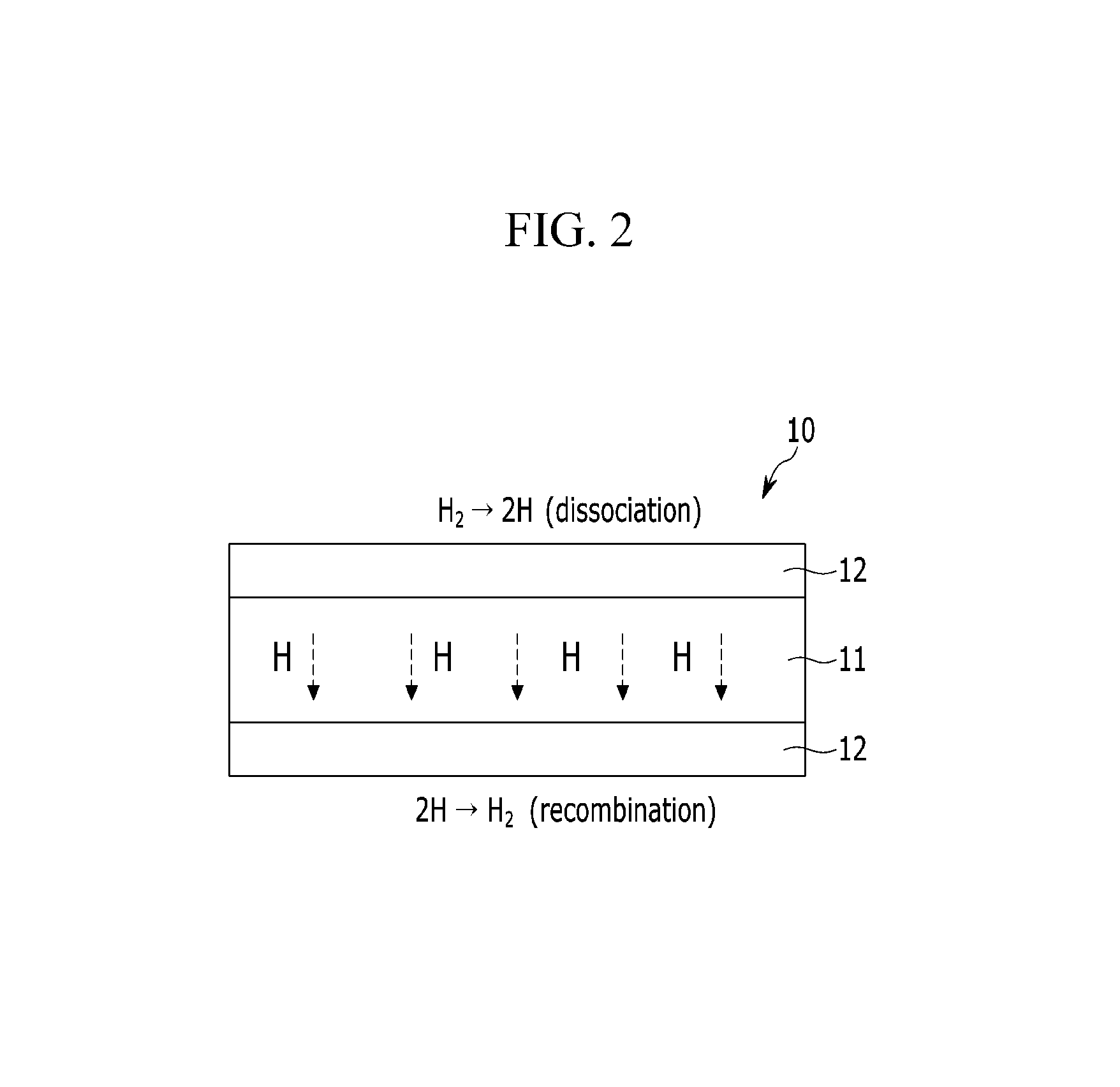
[0081]Nb and Ge metal are uniformly melted in an arc melting furnace to form an alloy, thus manufacturing a hydrogen separation membrane consisting of a separation membrane having a thickness of 50 micrometers (μm). Specifically, Nb at 95 atom % and Ge at 5 atom % are weighed to prepare a material, the arc melting furnace is purged with Ar gas and then evacuated to a high vacuum (5×10⁻⁵ torr or less) to prevent oxidation. An electrical current is increased to melt the Nb and Ge, and then the resulting alloy is sufficiently cooled. To manufacture a membrane having a desired thickness, the material is cold rolled and annealed to manufacture a separation membrane, and then thin Pd layers are formed on both sides of the membrane by rf sputtering process to a thickness of 200 nanometers (nm) to manufacture a hydrogen separation membrane.
example 2
[0082]A hydrogen separation membrane is manufactured by the same method as Example 1, except using a material prepared by weighing Nb at 90 atom % and Ge at 10 atom %.
example 3
[0083]V and Ge metal are uniformly melted in an arc melting furnace to form an alloy, thus manufacturing a hydrogen separation membrane consisting of a separation membrane having a thickness of 50 micrometers (μm). Specifically, V at 95 atom % and Ge at 5 atom % are weighed to prepare a material, the arc melting furnace is purged with Ar gas and then evacuated to a high vacuum (5×10⁻⁵ torr or less) to prevent oxidation. An electrical current is increased to melt the V and Ge, and then the resulting alloy is sufficiently cooled. To manufacture a membrane having a desired thickness, the material is cold rolled and annealed to manufacture a separation membrane, and then thin Pd layers are formed on both sides of the membrane by rf sputtering process to a thickness of 200 nanometers (nm) to manufacture a hydrogen separation membrane.
PUM
| Property | Measurement | Unit |
|---|---|---|
| thickness | aaaaa | aaaaa |
| 2θ | aaaaa | aaaaa |
| lattice constant | aaaaa | aaaaa |
Abstract
Description
Claims
Application Information


