Tunable nanoporous films on polymer substrates, and method for their manufacture

a technology of nanoporous films and polymer substrates, applied in the direction of vacuum evaporation coating, plasma technology, transportation and packaging, etc., can solve the problems of increasing the thickness of films made from stored solutions, requiring heating for both aging or condensing processes, and organic polysilica molecular weight. increase,

Active Publication Date: 2013-08-15
RENESSELAER POLYTECHNIC INST
View PDF3 Cites 35 Cited by
  • Summary
  • Abstract
  • Description
  • Claims
  • Application Information

AI Technical Summary

Benefits of technology

[0008]The adhesion of the nanoporous SiO2 to the polymer substrate allows for deposition on flexible and or moldable substrates while maintaining the optical and mechanical characteristics of the nanoporous film coating. These conformable coatings have many applications in the field of optics where the ability to fabricate tunable porosity coatings on a variety of materials and shapes is of great importance. The process can be extended to multi-layer films as well as a wide variety of deposited materials for additional applications.

Problems solved by technology

This process, like many of the previously employed methods of forming nanoporous films on semiconductors, has the disadvantage of requiring heating for both the aging or condensing process, and for the removal of a polymer to form the nanoporous film.
Furthermore, there is a disadvantage that organic polysilica tends to increase in molecular weight after the solution is prepared; consequently, the viscosity of such precursor solutions increases during storage, and the thickness of films made from stored solutions will increase as the age of the solution increases.
The instability of organic polysilica thus requires short shelf life, cold storage, and fine tuning of the coating parameters to achieve consistent film properties in a microelectronics / integrated circuit manufacturing process.

Method used


Image

  • Tunable nanoporous films on polymer substrates, and method for their manufacture
  • Tunable nanoporous films on polymer substrates, and method for their manufacture
  • Tunable nanoporous films on polymer substrates, and method for their manufacture

Examples


examples

[0090]The invention, having been generally described, may be more readily understood by reference to the following examples, which are included merely for purposes of illustration of certain aspects and embodiments of the present invention, and are not intended to limit the invention in any way.

[0091]Applicants conducted several experiments, demonstrating that tunable-porosity nanoporous coatings or films can be deposited on polymer substrates and that these nanoporous films have excellent adhesion to such substrates and preserve the optical and mechanical properties of the film.

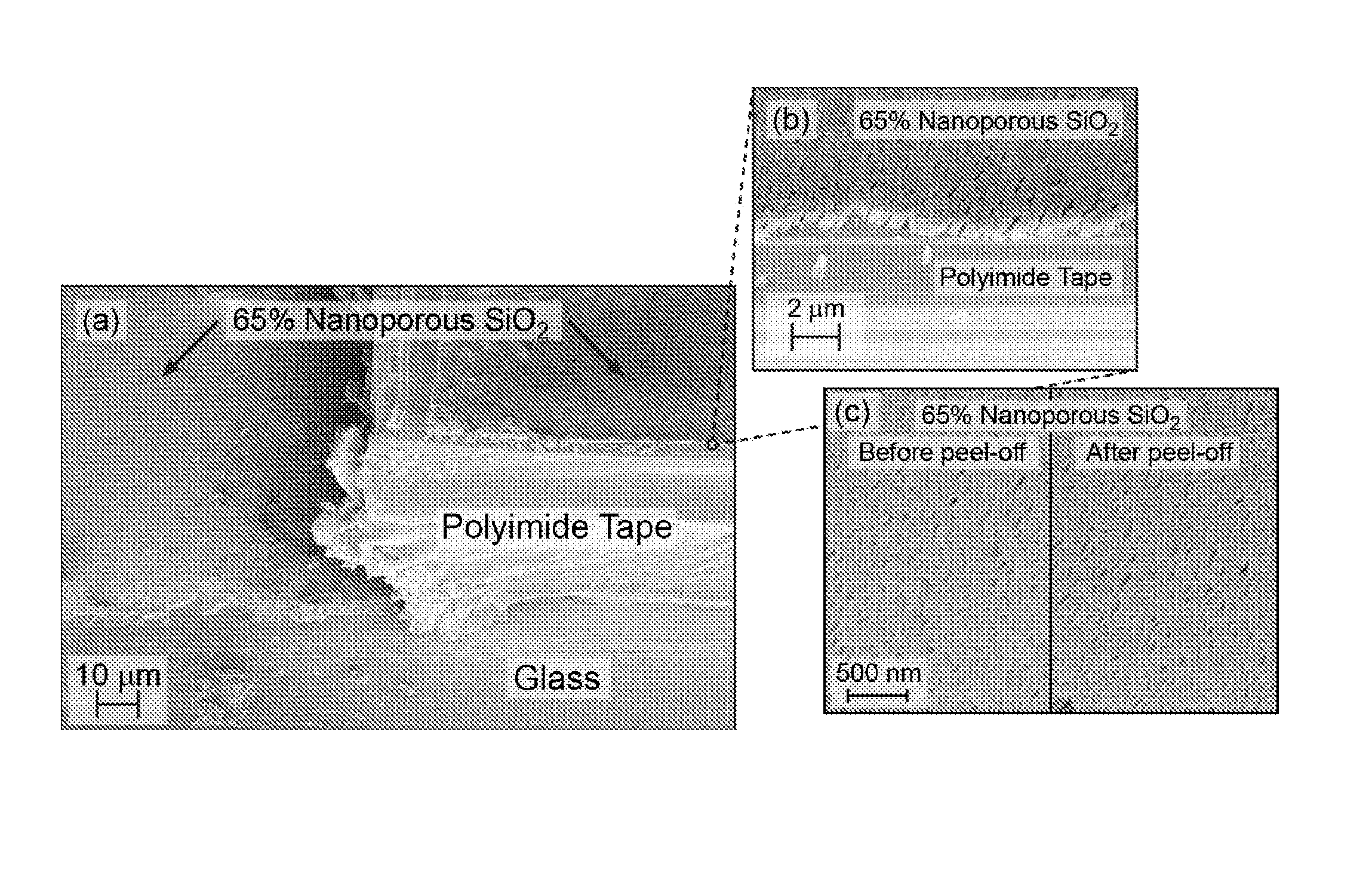
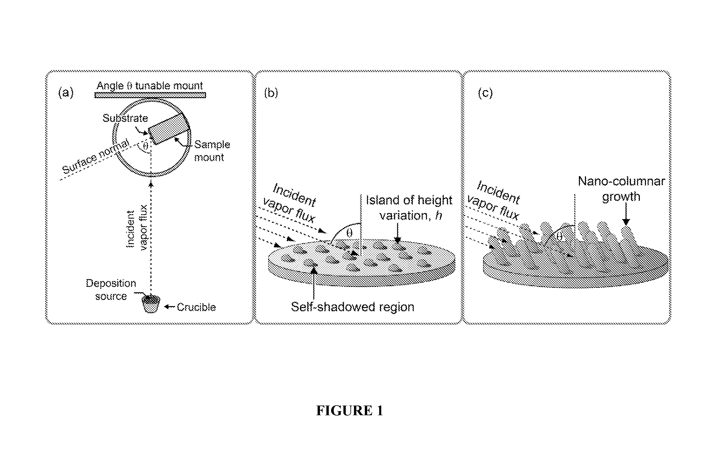
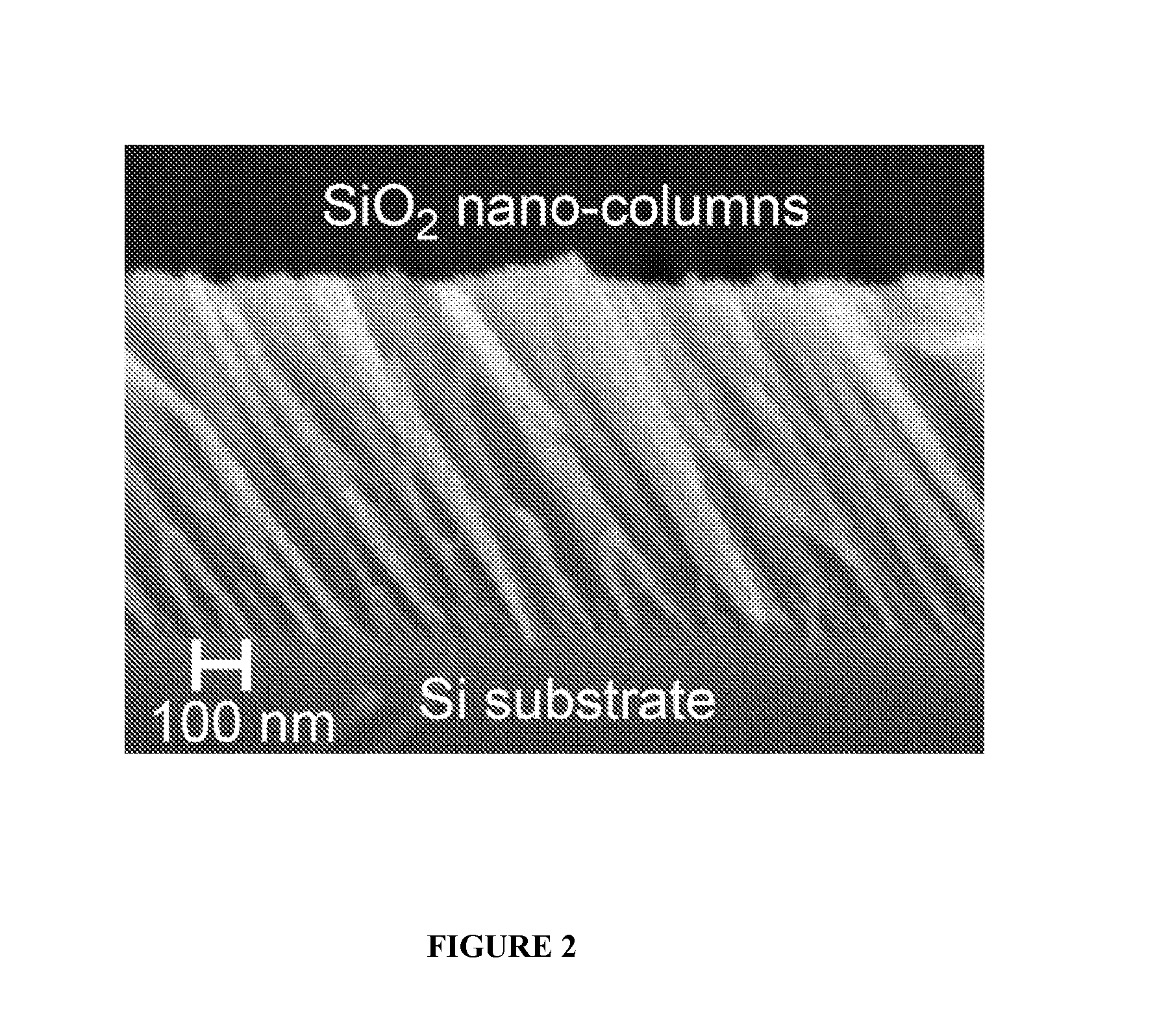
[0092]Using the method of fixed oblique-angle electron beam deposition, SiO2 and TiO2 nanoporous coatings of a variety of porosities and thicknesses were fabricated on various polymer substrates. A tilt-angle cross sectional SEM in FIG. 3a illustrates an example of such a nanoporous film fabricated on a polymer substrate (a 200 nm thick, 65% nanoporous SiO2 film was deposited on a Polyimide tape substrate) a...


PUM

PropertyMeasurementUnit
thickaaaaaaaaaa
thicknessaaaaaaaaaa
porosityaaaaaaaaaa

Abstract

The invention is directed to a composite polymer/nanoporous film system and methods of fabrication of tunable nanoporous coatings on flexible polymer substrates. The porosity of the nanoporous film can be tuned during fabrication to a desired value by adjusting the deposition conditions. Experiments show that SiO2 coatings with tunable porosity fabricated by oblique-angle electron beam deposition can be deposited on polymer substrates. These conformable coatings have many applications, including in the field of optics where the ability to fabricate tunable refractive index coatings on a variety of materials and shapes is of great importance.

Description

CROSS-REFERENCE TO RELATED APPLICATIONS[0001]This application claims the benefit of U.S. provisional patent application Ser. No. 61 / 402,174, filed Aug. 25, 2010, the entire disclosure of which is incorporated herein by reference.STATE AND FEDERAL FUNDED RESEARCH[0002]The invention described herein was made with support of the NYSTAR under Contract Number C090119. The U.S. Government may have certain rights to this invention.TECHNICAL FIELD[0003]The present invention relates generally to nanoporous films and polymer substrates, and related components, systems and methods. In one aspect, the present invention relates to nanoporous coatings on flexible or moldable polymer substrates.BACKGROUND OF THE INVENTION[0004]A variety of coating compositions have been reported for several decades. More recently, however, advances in fabrication and characterization methods of nanostructured films have helped spark renewed interest of these films for use in a wide range of applications. The drive...

Claims


Application Information

Patent Timeline
Patent Type & Authority Applications(United States)
IPC IPC(8): C23C16/48C23C14/32C23C14/34C23C16/44C23C16/50
CPCB82Y20/00B82Y30/00C23C14/083C23C14/10C23C14/226C23C16/50C23C14/325C23C14/34C23C16/44C23C16/487Y02T50/67Y10T428/249967Y10T428/249969Y10T428/24997Y10T428/249978Y02T50/60
Inventor POXSON, DAVID J.MONT, FRANK W.SCHUBERT, E. FREDSIEGEL, RICHARD W.
Owner RENESSELAER POLYTECHNIC INST
Why Eureka
Try Eureka