Light emitting component and light emitting device using same

Active Publication Date: 2013-08-22
EPISTAR CORP
View PDF23 Cites 15 Cited by
  • Summary
  • Abstract
  • Description
  • Claims
  • Application Information

AI Technical Summary

Benefits of technology

[0007]To overcome the problems, light emitting devices must comprise circuit to control the light emitting diodes and maintain the reliability and efficiency. Therefore, more and more electronic components are incorporated in the devices, and integration or hybrid technologies are developed. A field effect transistor (FET) is one of examples which may be manufactured using semiconductor epitaxy technology, as disclosed in U.S. Pat. Nos. 7,432,538, 7,750,351 and 7,981,744. However, these patents were failed to di

Problems solved by technology

However, these patents were failed to disclose how to incorporate with an LED and related application.
However, the process of Deschler'

Method used


Image

  • Light emitting component and light emitting device using same
  • Light emitting component and light emitting device using same
  • Light emitting component and light emitting device using same

Examples


first embodiment

The First Embodiment

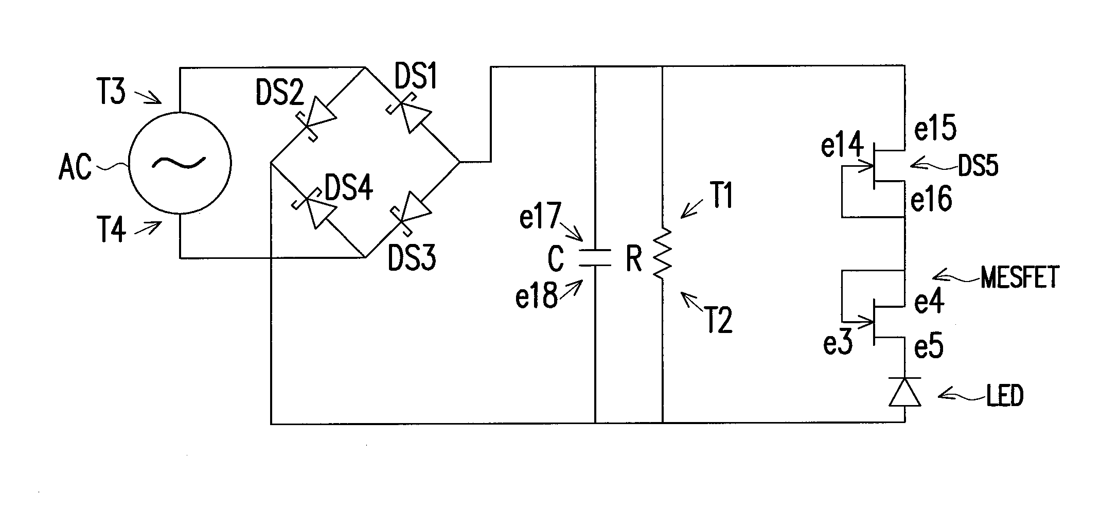
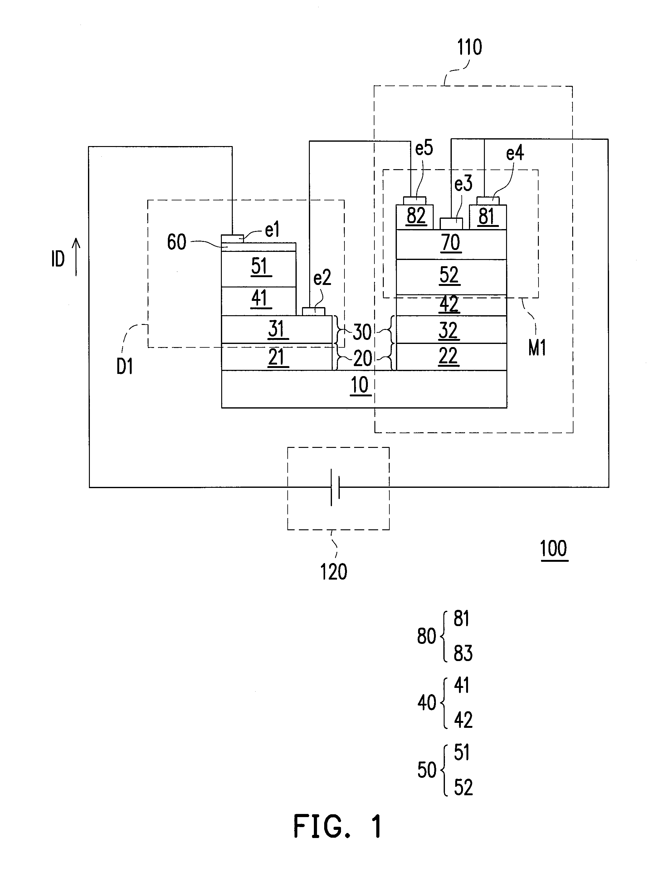
[0043]FIG. 1 is a physical schematic diagram of a light emitting device 100 according to an embodiment of the present invention. Referring to FIG. 1, the light emitting device 100 includes a current stabilizing unit 110, a power source 120, and a diode D1, wherein the diode D1 is a light emitting diode and formed on a growth substrate 10. The growth substrate 10 is, for example, a sapphire substrate commonly used for forming light emitting diodes. In a manufacturing process for a light emitting diode (LED), the LED may typically comprise layers such as a buffer layer 20, a first type semiconductor layer 30, an active layer 40, a second type semiconductor layer 50 and a transparent conductive layer (TCL) 60. The buffer layer 20 is normally formed of, for example, aluminum nitride (AlN). The first type semiconductor layer 30 may be an n-type III-nitride such as an n-type gallium nitride (n-GaN), an n-type aluminum gallium nitride (n-AlGaN), or an n-type indium gall...

second embodiment

The Second Embodiment

[0074]FIG. 12 is a schematic diagram of a light emitting device according to an embodiment of the present invention. Referring to FIG. 12, a light emitting device 2000 in the present embodiment includes a growth substrate S1, a first type semiconductor layer 100A, an active layer AL formed on top of the first type semiconductor layer 100A, a second type semiconductor layer 200A formed on top of the active layer AL, a third type semiconductor layer 300A formed on top of the second type semiconductor layer 200A, and a fourth type semiconductor layer 400A formed on top of the third type semiconductor layer 300A. In the present embodiment, the growth substrate S1 may be a sapphire substrate, GaN substrate or Si substrate for example, and yet the present invention is not limited thereto. In the present embodiment, materials of the first type semiconductor layer 100A, the second type semiconductor layer 200A, the third type semiconductor layer 300A, and the fourth typ...

third embodiment

The Third Embodiment

[0096]FIG. 21 is a schematic diagram of a light emitting device according to an embodiment of the present invention. Referring to FIG. 21, a light emitting device 3000 of the present invention includes a growth substrate S1, a first type semiconductor layer 100B, a second type semiconductor layer 200B formed on top of the first type semiconductor layer 100B, a third type semiconductor layer 300B formed on top of the second type semiconductor layer 200B, and a fourth type semiconductor layer 400B formed on top of the third type semiconductor layer 300B. In the present embodiment, a first semiconductor region 401b, a source semiconductor region 402b and a drain semiconductor region 403b are separated from the fourth type semiconductor layer 400B. An active layer AL is formed on top of the first semiconductor region 401b, and a second semiconductor region 500B is formed on top of the active layer AL. A third semiconductor region 301b and a channel semiconductor regi...


PUM


Abstract

A light emitting device including a light emitting component is provided, wherein said light emitting comprising an integrated light emitting diode and a semiconductor field effect transistor. The semiconductor field effect transistor may prevent situations such as overheating and voltage instability by controlling a current passing through the light emitting diode as well as enhancing the ability to withstand electrostatic discharge and reducing cost of the light emitting device in multiple aspects.

Description

CROSS-REFERENCE TO RELATED APPLICATION[0001]This application claims the priority benefits of Taiwan application serial no. 101105652, filed on Feb. 21, 2012, and Taiwan application serial no. 101142263, filed on Nov. 13, 2012. The entirety of each of the above-mentioned patent applications is hereby incorporated by reference herein and made a part of this specification.BACKGROUND OF THE INVENTION[0002]1. Field of the Invention[0003]The present invention generally relates to a light emitting component, in particular, to a light emitting component comprising an integrated light emitting diode and a semiconductor field effect transistor, and a light emitting device using same.[0004]2. Description of Related Art[0005]Semiconductor light emitting diodes (LEDs) have many advantages and possess characteristics of long lifetime, power saving, low contamination, compact and lightweight form factor, low fragility, high switching speed, and high reliability at normal temperatures, therefore li...

Claims


Application Information

Patent Timeline
IPC IPC(8): H05B37/02H01L33/00H05B44/00
CPCH01L27/15H05B37/02H01L33/0025H05B33/0815H01L27/0629H01L29/872H05B33/0824H05B45/44Y02B20/30H05B45/395
Inventor HUANG, CHIH-SHUTUN, CHUN-JUPAN, SHYI-MINGCHENG, WEI-KANGLIAO, KENG-YING
Owner EPISTAR CORP
Why Eureka
Try Eureka