Light emitting diode and a manufacturing method thereof, a light emitting device

a technology of light emitting diodes and manufacturing methods, applied in the field of semiconductor technology, can solve the problems of low luminous efficiency of semiconductor light emitting diodes in the prior art, energy waste, and inability to be used inside the device, and achieve the effect of high luminous efficiency

Inactive Publication Date: 2013-08-29
ENRAYTEK OPTOELECTRONICS
View PDF4 Cites 1 Cited by
  • Summary
  • Abstract
  • Description
  • Claims
  • Application Information

AI Technical Summary

Benefits of technology

[0006]An object of the present invention is to provide a light emitting diode having high luminous efficiency.

Problems solved by technology

However, semiconductor light emitting diodes have low luminous efficiency in the prior art.
A lot of energy inside the device can not be sent out, thereby not only causing energy waste, but also affecting lifetime of the device.
However, the method disclosed in this prior art needs to form a film comprising a plurality of high refractive index layers and low refractive index layers stacked on the substrate, of which the manufacturing process is very complex.

Method used


Image

  • Light emitting diode and a manufacturing method thereof, a light emitting device
  • Light emitting diode and a manufacturing method thereof, a light emitting device
  • Light emitting diode and a manufacturing method thereof, a light emitting device

Examples


Embodiment Construction

[0018]Hereunder, the present invention will be described in detail with reference to embodiments, in conjunction with the accompanying drawings.

[0019]Although the present invention has been disclosed hereinafter as above with reference to preferred embodiments in details, the present invention can be implemented in other embodiments which are different. Therefore, the present invention should not be limited to the embodiments disclosed here.

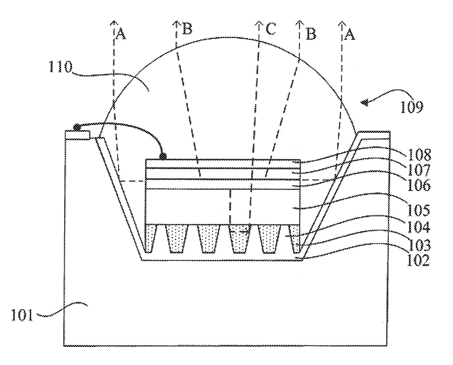
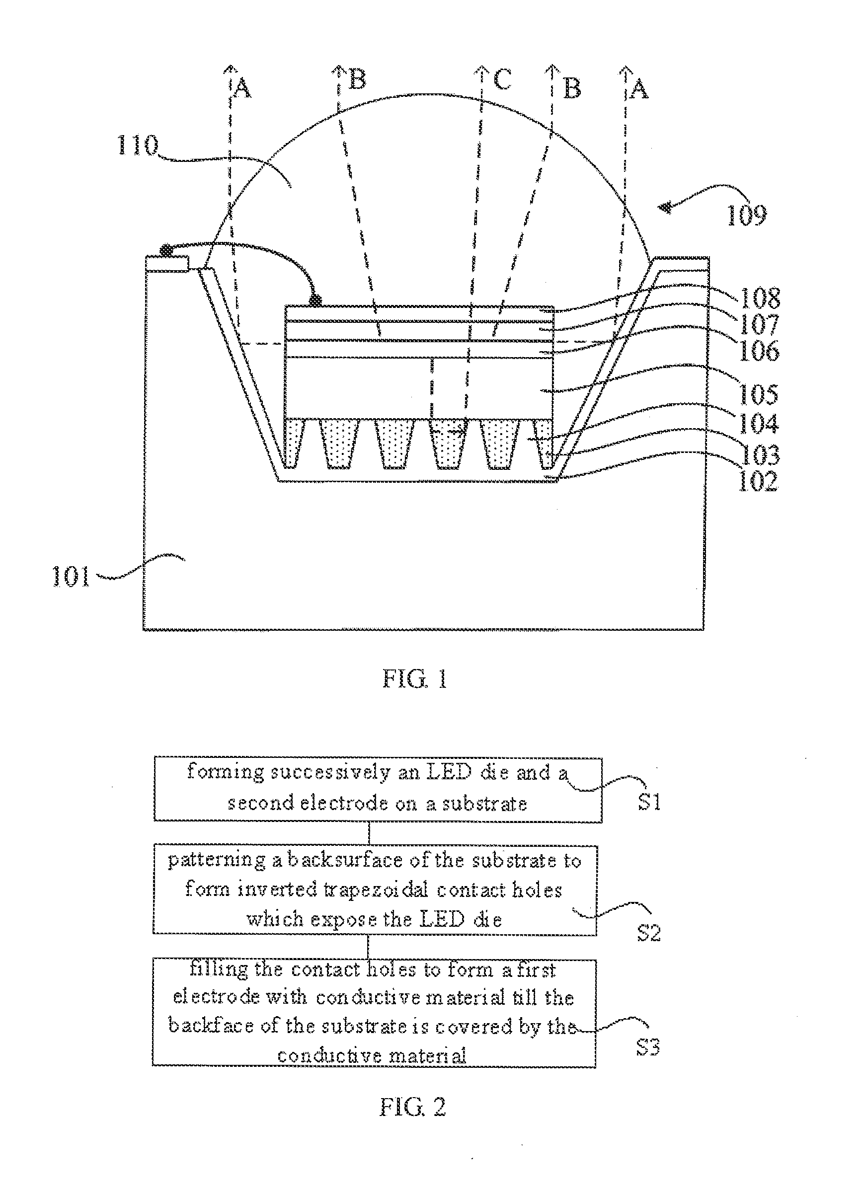
[0020]As taught in the background of the invention, in order to improve the luminous efficiency of semiconductor light emitting diodes, the method disclosed in the prior art needs to form a film comprising a plurality of high refractive index layers and low refractive index layers stacked on the substrate, and the production process of the film is very complex.

[0021]In order to solve this problem, the present invention provides a light emitting device comprising a light emitting diode. The light emitting diode comprises: a first electrode adapted...


PUM


Abstract

The present invention provides an LED and the manufacturing method thereof, and a light emitting device. The LED includes a first electrode, for connecting the LED to a negative electrode of a power supply; a substrate, located on the first electrode; and an LED die, located on the substrate; in which a plurality of contact holes are formed extending through the substrate, the diameter of upper parts of the contact holes is less than the diameter of lower parts of the contact holes, and the contact holes are filled with electrode plugs connecting the first electrode to the LED die. The light emitting device includes the LED, and further includes a susceptor and an LED mounted on the susceptor. The manufacturing method includes: forming successively an LED die and a second electrode on a substrate; patterning a backsurface of the substrate to form inverted trapezoidal contact holes which expose the LED die; and filling the contact holes with conductive material till the backface of the substrate is covered by the conductive material. The LED has a high luminous efficiency and the manufacturing method is easy to implement.

Description

CROSS REFERENCE TO RELATED APPLICATIONS[0001]The present application claims the priority of Chinese Patent Application No. 201010538428.3, entitled “A light emitting diode and a manufacturing method thereof, a light emitting device”, and filed Nov. 9, 2010, the entire disclosure of which is incorporated herein by reference.FIELD OF THE INVENTION[0002]The present invention relates to semiconductor technology, and particularly relates to a light emitting diode and a manufacturing method thereof, and a light emitting device.BACKGROUND OF THE INVENTION[0003]A light emitting diode (LED) is a semiconductor device which is activated by current to generate light of various colors. The III-V compound semiconductors, such as gallium nitride (GaN), which have wide band gap, high luminous efficiency, high electron saturation drift velocity, and stable chemical properties, have great application potential in high-brightness blue light emitting diodes, blue laser and other optoelectronic devices ...

Claims


Application Information

Patent Timeline
Patent Type & Authority Applications(United States)
IPC IPC(8): H01L33/38
CPCH01L33/20H01L33/382H01L2933/0016H01L33/46H01L33/38H01L2933/0091
Inventor CHANG, RICHARD RUGINXIAO, DEYUAN
Owner ENRAYTEK OPTOELECTRONICS
Why Eureka
Try Eureka