Method for manufacturing group iii nitride semiconductor light-emitting element, group iii nitride semiconductor light-emitting element, lamp, and reticle

a technology of nitride and semiconductor light-emitting elements, which is applied in the direction of instruments, originals for photomechanical treatment, optics, etc., can solve the problems of adverse effects on light-emitting properties, suppress the occurrence of deformation or deficiency of convex portions in the substrate, improve the external appearance properties of light-emitting elements, and improve crystallinity

Active Publication Date: 2013-08-29
TOYODA GOSEI CO LTD
View PDF9 Cites 6 Cited by
  • Summary
  • Abstract
  • Description
  • Claims
  • Application Information

AI Technical Summary

Benefits of technology

[0043]According to the method for manufacturing the Group III nitride semiconductor light-emitting element of the invention, the method including the substrate-processing process of forming the main surface including the flat surface and the convex portions in the substrate is adopted In the substrate-processing process, the mask patterns are sequentially formed in the respective regions of the flat surface, which is formed from the (0001) C-plane, of the substrate using the polygonal reticle having two pairs of parallel opposing ends in a plan view by the stepper exposure method. Then, the flat surface is etched. According to this, in an in-plane direction of the flat surface of the substrate, the plurality of the convex portions are arranged to be parallel with the two pairs of parallel ends of the reticle, respectively, and to be periodic in two axial directions of one arrangement axis and the other arrangement axis intersecting each other. In addition, among the plurality of convex portions, three arbitrary convex portions, which are adjacent to each other and are arranged in a triangular shape in a plan view, are disposed in an isosceles triangular shape in a plan view. When the method including the above-described substrate-processing process is adopted, occurrence of deformation or deficiency of the convex portions in the substrate may be suppressed, and at the same time, a linear convex portion may be prevented from being generated in the substrate. According to this, occurrence of a partial modification in each layer, which is formed on the main surface of the substrate, may be suppressed, and thus external appearance properties of the light-emitting element are improved, and occurrence of dislocation in each layer of the LED structure formed on the Group III nitride semiconductor layer is suppressed. Accordingly, the crystallinity is improved, and thus the internal quantum efficiency is improved. In addition, when the deformation or deficiency of the convex portions is suppressed, the light confinement inside the light-emitting element due to scattered reflection of light is reduced. As a result, the light extraction efficiency is improved.
[0044]Accordingly, the Group III nitride semiconductor light-emitting element, in which the internal quantum efficiency and the light extraction efficiency are high, and which has excellent light-emitting properties and external appearance properties, may be manufactured with high productivity.
[0045]In addition, since the Group III nitride semiconductor light-emitting element of the invention is obtained according to the method for manufacturing the Group III nitride semiconductor light-emitting element of the invention, according to the Group III nitride semiconductor light-emitting element of the invention, the internal quantum efficiency and the light extraction efficiency are high, and thus excellent light-emitting properties may be obtained.
[0046]Furthermore, since the Group III nitride semiconductor light-emitting element of the invention is used, the lamp related to the invention has excellent light-emitting properties.

Problems solved by technology

In addition, when an element is formed, light-emitting properties are adversely affected.

Method used


Image

  • Method for manufacturing group iii nitride semiconductor light-emitting element, group iii nitride semiconductor light-emitting element, lamp, and reticle
  • Method for manufacturing group iii nitride semiconductor light-emitting element, group iii nitride semiconductor light-emitting element, lamp, and reticle
  • Method for manufacturing group iii nitride semiconductor light-emitting element, group iii nitride semiconductor light-emitting element, lamp, and reticle

Examples


example 1

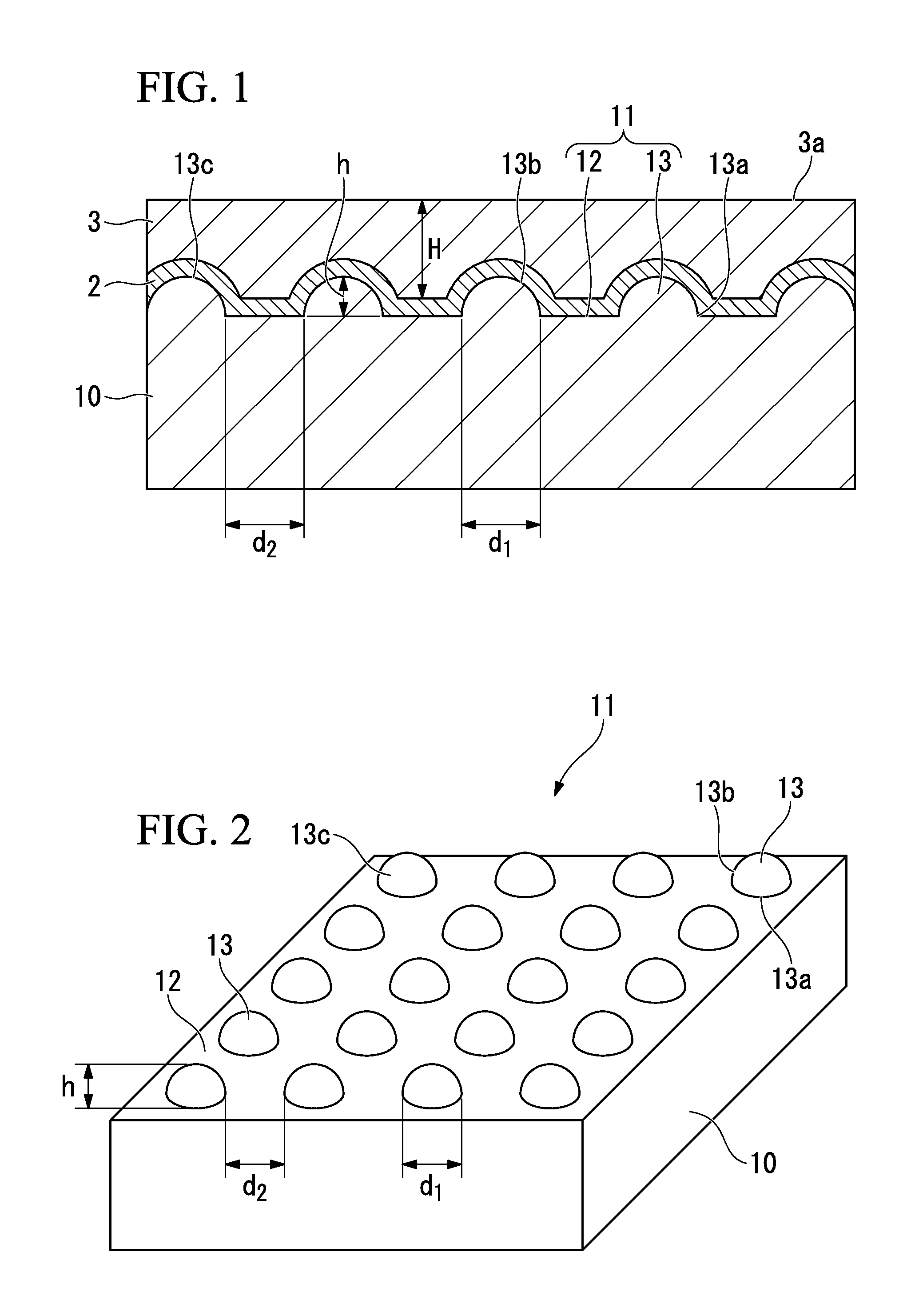
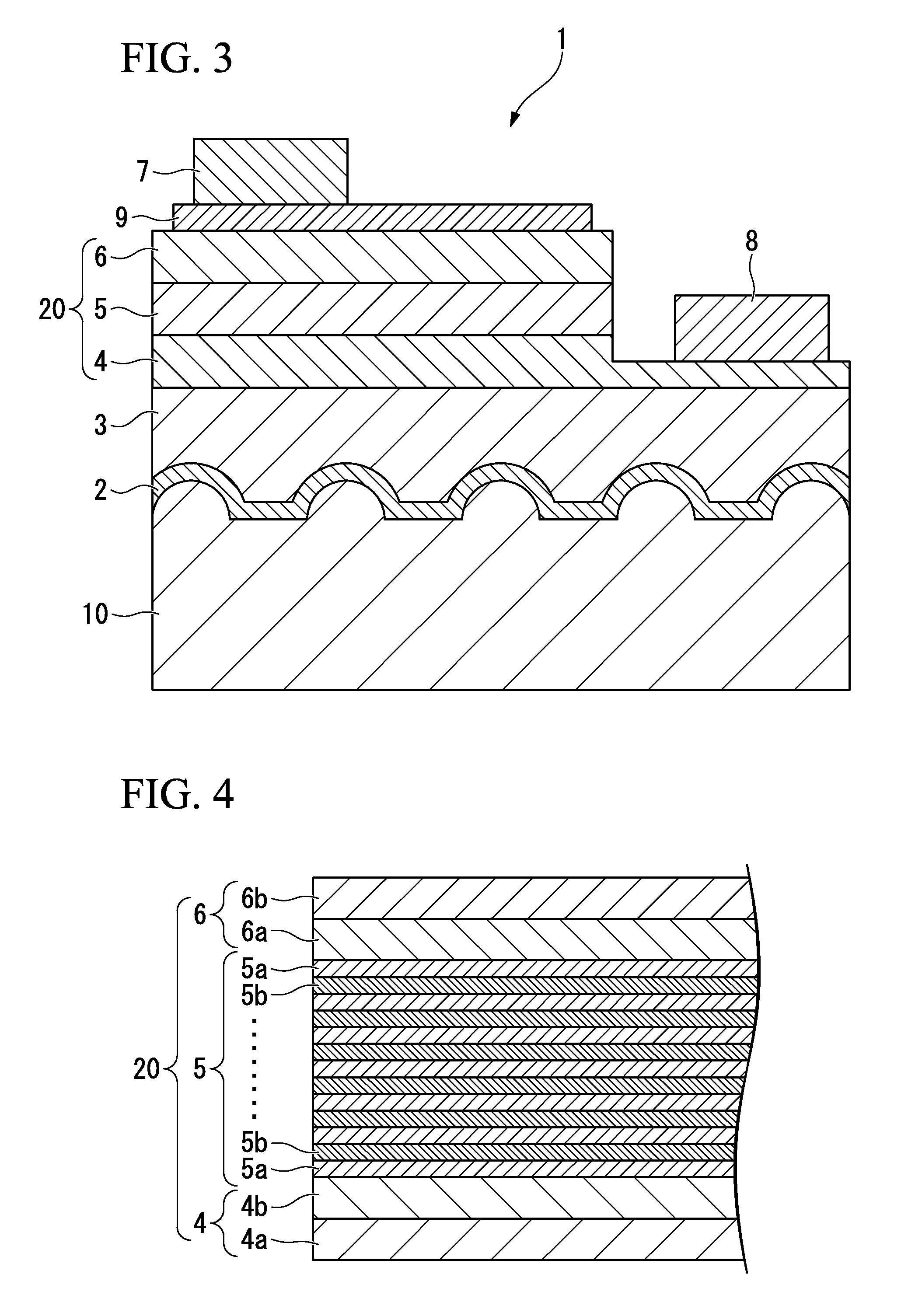
[0194]First, a plurality of convex portions, which were set to conditions shown in Table 1 to be described below, were formed in the (0001) C-plane of a sapphire substrate in the following sequences, whereby a substrate having a main surface including a flat surface and convex portions was prepared (substrate-processing process). That is, a mask was formed on the C-plane sapphire substrate having the diameter of four inches by a photolithography method, and the sapphire substrate was etched by a dry etching method, whereby the convex portions were formed in the sapphire substrate.

[0195]In addition, in the substrate-processing process, a stepper exposure method using ultraviolet light was used as an exposure method during formation of the mask pattern on the substrate. In addition, as a reticle (photomask) provided to a stepper exposure apparatus, a reticle was used which was set to a parallelogram shape in a plan view, and in which dots configured to pattern a held resist were provi...

example 2

[0212]In Example 2, a substrate having the main surface including the flat surface and the convex portions having the conditions shown in Table 1 was prepared in the same sequence as Example 1 except that as the reticle, a reticle was used which had a parallelogram shape in a plan view, and in which a cut-out portion was formed at one corner portion among corner portions of the reticle as shown in FIG. 7 and Table 1. Then, the buffer layer and the underlying layer were laminated on the substrate. At this time, the mask patterns were formed on the surface of the substrate while moving the reticle in such a manner that a position of the cut-out portion of the reticle and a position of at least one corner portion among the corner portions of the reticle after the movement overlap each other during sequential movement of the reticle on the substrate according to the stepper exposure method. In addition, a half-value width of X-ray diffraction (XRD) of a (10-10) plane and a (0002) plane ...

examples 3 and 4

[0216]In Examples 3 and 4, a substrate having the main surface including the flat surface and the convex portions having the conditions shown in Table 1 was prepared in the same sequence as Example 2 except that one side of the reticle having a parallelogram shape in a plan view as shown in FIG. 7 was inclined with respect to the orientation flat of the substrate at an angle shown in Table 1. Then, the buffer layer and the underlying layer were laminated on the substrate. At this time, the mask patterns were formed on the surface of the substrate while moving the reticle in such a manner that a position of the cut-out portion of the reticle and a position of at least one corner portion among the corner portions of the reticle after the movement overlap each other during sequential movement of the reticle on the substrate according to the stepper exposure method. In addition, the half-value width of X-ray diffraction (XRD) of the (10-10) plane and the (0002) plane of the underlying l...


PUM

PropertyMeasurementUnit
vertex angleaaaaaaaaaa
angleaaaaaaaaaa
heightaaaaaaaaaa

Abstract

A method for manufacturing a Group III nitride semiconductor light-emitting element of the invention includes a substrate-processing process of forming a main surface including a flat surface and a convex portion 13 on the substrate 10, an epitaxial process of epitaxially growing an underlying layer on the main surface of the substrate 10 so as to cover the flat surface and the convex portion 13, and an LED lamination process of forming an LED structure by epitaxially growing a Group III nitride semiconductor. In the substrate-processing process, mask patterns 15 are sequentially formed in respective regions R1 and R2 of the flat surface using a polygonal reticle 51 having two pairs of parallel opposing ends in a plan view, by a stepper exposure method, and then the flat surface is etched to dispose and form three arbitrary convex portions 13, which are arranged to be adjacent to each other, in an isosceles triangular shape in a plan view.

Description

BACKGROUND OF THE INVENTION[0001]1. Field of the Invention[0002]The present invention relates to a method for manufacturing a Group III nitride semiconductor light-emitting element having a light-emitting diode (LED) structure, a Group III nitride semiconductor light-emitting element, a lamp, and a reticle that is used for the manufacturing of the Group III nitride semiconductor light-emitting element.[0003]Priority is claimed on Japanese Patent Application No. 2012-038612, filed on Feb. 24, 2012, the content of which is incorporated herein by reference.[0004]2. Description of Related Art[0005]In recent years, as a semiconductor material for a light-emitting element that emits light with a short wavelength, a Group III nitride semiconductor has attracted attention. The Group III nitride semiconductor is expressed by a general formula AlxGayInzN (0≦x≦1, 0≦y≦1, 0≦z≦1, and x+y+z=1), and is formed on a substrate formed from various oxides such as a sapphire single crystal or Group III-V...

Claims


Application Information

Patent Timeline
Patent Type & Authority Applications(United States)
IPC IPC(8): H01L33/06G03F1/00
CPCH01L33/007H01L21/0237H01L21/0242H01L21/0243H01L21/02458Y10S438/943H01L33/06G03F1/00H01L21/0334H01L33/0075H01L21/0254
Inventor TANAKA, KAZUFUMI
Owner TOYODA GOSEI CO LTD
Why Eureka
Try Eureka