

Trench isolation structure and method for forming the same
a technology of isolation structure and divot, which is applied in the direction of basic electric elements, electrical apparatus, and semiconductor devices, can solve the problems of leakage and device performance degradation, and more device performance degradation, so as to reduce the impact of the divot on the performance of the semiconductor device, and reduce the size of the divot
- Summary
- Abstract
- Description
- Claims
- Application Information
AI Technical Summary
Benefits of technology
Problems solved by technology
Method used
Image

Examples
first embodiment
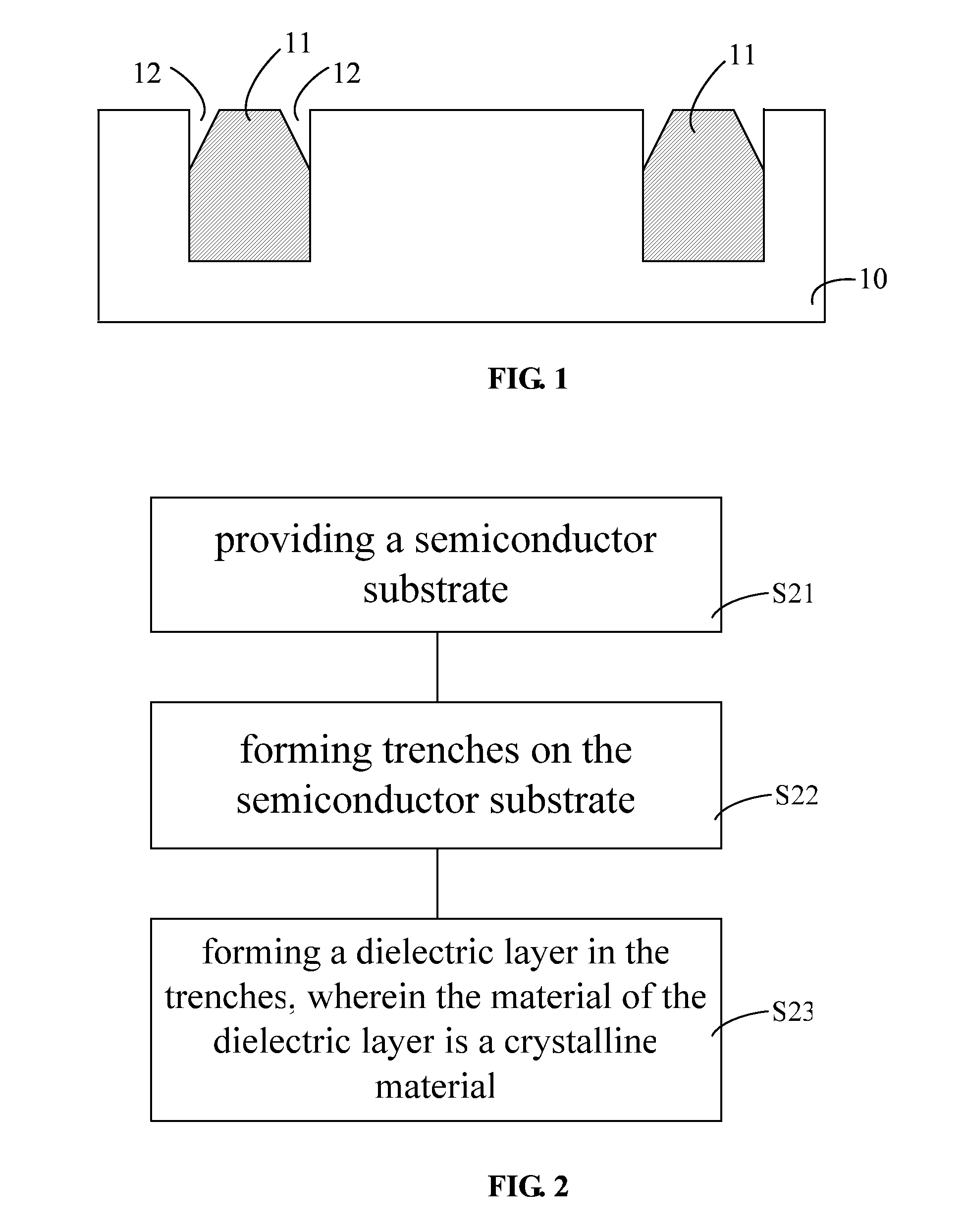
[0044]FIG. 2 is a flow chart of a method for forming a trench isolation structure according to the present invention. As shown in FIG. 2, the method includes:
[0045]step S21: providing a semiconductor substrate;
[0046]step S22: forming trenches on the semiconductor substrate; and
[0047]step S23: forming a dielectric layer in the trenches, wherein the material of the dielectric layer is a crystalline material.
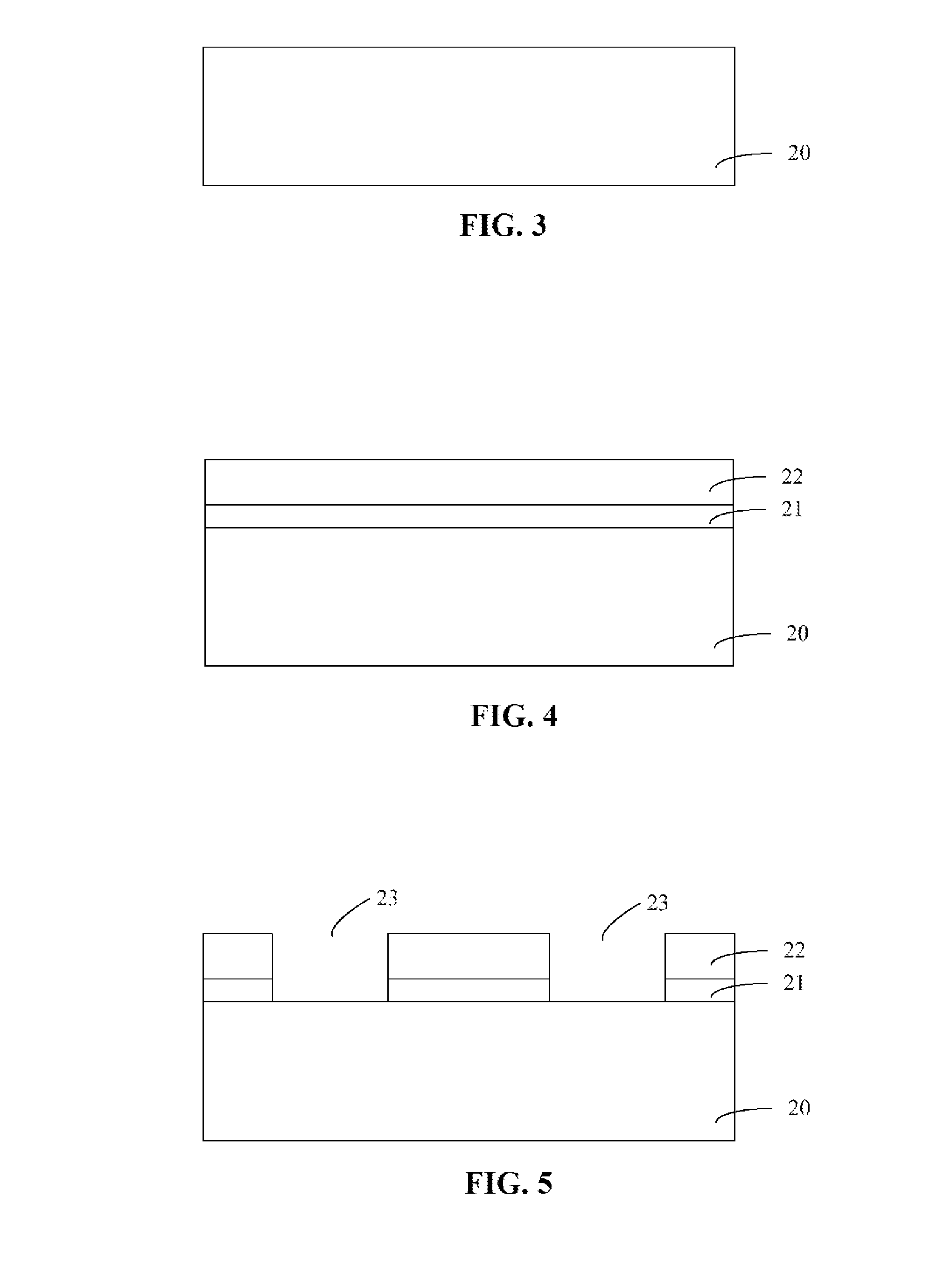
[0048]FIGS. 3-8 illustrate a method for forming a trench isolation structure according to a first embodiment of the present invention with sectional views of intermediate structures. The embodiment is described below with reference to FIGS. 2 and 3-8.
[0049]With reference to FIGS. 2 and 3, step S21 is performed: providing a semiconductor substrate. In particular, a semiconductor substrate 20 is provided, and the semiconductor substrate 20 may be a silicon substrate, a silicon-germanium substrate, a III-V compound substrate (e.g., gallium arsenide, indium phosphide, or gallium nitrid...
second embodiment
[0060]FIG. 10 shows a cross-sectional view of a trench isolation structure formed according to the present invention. The trench isolation structure includes: a semiconductor substrate 30, and trenches formed on the semiconductor substrate 30 and filled with a dielectric layer 31, wherein the material of the dielectric layer 31 is a crystalline material. In particular, the dielectric layer 31 has a multi-layer structure including a first dielectric layer 31a and a second dielectric layer 31b. Of course, in other embodiments, the dielectric layer 31 may include more dielectric layers, e.g., three layers or four layers. Impurity ions may be introduced into the dielectric layer 31 such that the lattice constant of the dielectric layer 31 is larger or smaller than the lattice constant of the semiconductor substrate 30. A MOS transistor may be formed on the semiconductor substrate 30 between the trenches. The MOS transistor may include a gate stack 32, and a source and a drain in the sem...
third embodiment
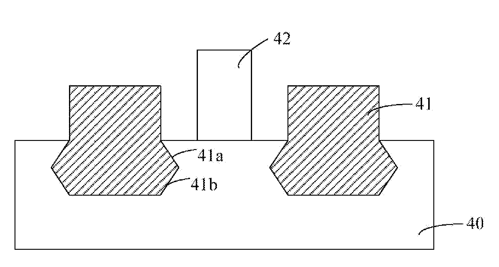
[0061]FIG. 11 shows a cross-sectional view of a trench isolation structure formed according to the present invention. The trench isolation structure includes: a semiconductor substrate 40, and trenches formed on the semiconductor substrate 40 and filled with a dielectric layer 41, wherein the material of the dielectric layer 41 is a crystalline material. In particular, the sidewalls of the trench form a diamond shape and include an upper sidewall 41a and a lower sidewall 41b connected with each other. The upper sidewall 41a and the lower sidewall 41b are in the {111} lattice plane of the semiconductor substrate 40 Impurity ions may be introduced into the dielectric layer 41 such that the lattice constant of the dielectric layer 41 is larger or smaller than the lattice constant of the semiconductor substrate 40. A MOS transistor may be formed on the semiconductor substrate 40 between the trenches. The MOS transistor may include a gate stack 42, and a source and a drain in the semicon...
PUM
 Abstract
Description
Claims
Application Information