Semiconductor laminate, semiconductor device, and production method thereof

a semiconductor and semiconductor technology, applied in the field of semiconductor devices and semiconductor laminates, can solve the problems of limited application, inadequate durability in air stability, and inability to meet the requirements of use, and achieve favorable semiconductor properties, favorable semiconductor properties, and favorable semiconductor properties

Inactive Publication Date: 2013-09-05
TEIJIN LTD
View PDF3 Cites 191 Cited by
  • Summary
  • Abstract
  • Description
  • Claims
  • Application Information

AI Technical Summary

Benefits of technology

[0302]In a semiconductor device obtained by the method of the present invention and the semiconductor device of the present invention, in the case where the crystal orientation of a dopant injection layer is the same as the crystal orientation of a semiconductor layer or substrate, entrapment of a carrier at the interface between the dopant injection layer and the semiconductor layer or substrate composed of a semiconductor element can be inhibited.
[0303]In addition, in a semiconductor device obtained by the method of the present invention and the semiconductor device of the present invention, in the case where the concentration of dopant at a depth of 0.1 μm from the surface of a first dopant injection layer is 1×10²⁰ atoms / cm3 or more, and the dopant concentration at a depth of 0.3 μm, and particularly a depth of 0.2 μm from the surface of the first dopant injection layer is 1 / 10 or less of the dopant concentration at a depth of 0.1 μm, namely in the case where the doped concentration gradient is high and thereby a high doped concentration is reached while reducing the thickness of the highly doped portion, light absorption by the high dopant concentration layer can be inhibited, and properties obtained when the high dopant concentration layer is used as a back surface electric field layer or front surface electric field layer can be improved.
[0304]In addition, the dispersion of the present invention can be preferably used as the method of the present invention.Effects of Second Present Invention
[0305]According to the green silicon particle film of the present invention having a low content of desorbing gas, a semiconductor silicon film having favorable semiconductor properties can be provided by sintering the green silicon particle film with light irradiation or heating. In addition, in the case of having sintered this green silicon particle film by irradiating with light, a semiconductor silicon film having favorable semiconductor properties can be provided without using a relatively high temperature.
[0306]According to the semiconductor silicon film of the present invention having a low carbon content, favorable semiconductor properties can be provided.
[0307]According to the method of the present invention, the green silicon particle film and semiconductor silicon film of the present invention can be obtained.Effects of Third Present Invention

Problems solved by technology

However, organic semiconductor films have inadequate performance in terms of carrier mobility as well as inadequate durability in terms of stability in air in comparison with silicon semiconductor films.
These problems place limitations on their applications, and makes commercialization thereof difficult.
However, since inorganic compound semiconductor materials such as InGaZnO4 have problems with raw material availability, they are extremely expensive in comparison with silicon semiconductors, and are not practical for use as typical TFT materials.
This makes it difficult to lower the temperature of the overall process.

Method used


Image

  • Semiconductor laminate, semiconductor device, and production method thereof
  • Semiconductor laminate, semiconductor device, and production method thereof
  • Semiconductor laminate, semiconductor device, and production method thereof

Examples


examples

First Present Invention

example a1

Fabrication of Boron (B)-Doped Silicon Particles

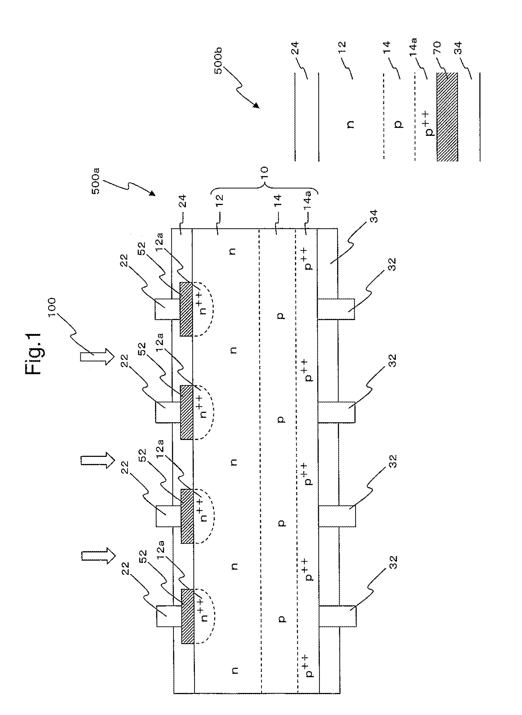
[0776]Silicon particles were fabricated by laser pyrolysis (LP) using a carbon dioxide (CO2) laser and using monosilane (SiH4) gas as the raw material. At this time, B2H6 gas was introduced together with the SiH4 gas to obtain boron-doped silicon particles.

[0777]The doping concentration of the resulting boron-doped silicon particles was 1×10²¹ atoms / cm3. In addition, the mean primary particle diameter of the resulting boron-doped silicon particles was about 5.5 nm (maximum particle diameter: 15 nm, minimum particle diameter: 2 nm), and the value of variance was 6 nm. In addition, the degree of crystallization of the resulting boron-doped silicon particles was 5%.

[0778](Preparation of Dispersion)

[0779]Boron-doped silicon particles obtained in the above manner were ultrasonically dispersed in isopropyl alcohol (IPA) to obtain a silicon particle dispersion having a solid fraction concentration of 2% by weight.

[0780](Preparation of Substra...

example a2

Fabrication of Phosphorous (P)-Doped Silicon Particles

[0804]Silicon particles were fabricated by laser pyrolysis (LP) using a carbon dioxide (CO2) laser and using monosilane (SiH4) gas as the raw material. At this time, PH3 gas was introduced together with the SiH4 gas to obtain phosphorous-doped silicon particles.

[0805]The doping concentration of the resulting phosphorous-doped silicon particles was 1×10²¹ atoms / cm3. In addition, the mean primary particle diameter of the resulting phosphorous-doped silicon particles was about 8.0 nm (maximum particle diameter: 16 nm, minimum particle diameter: 4 nm), and the value of variance was 4.3 nm. In addition, the degree of crystallization of the resulting phosphorous-doped silicon particles was 12%.

[0806](Preparation of Dispersion)

[0807]Phosphorous-doped silicon particles obtained in the above manner were ultrasonically dispersed in isopropyl alcohol (IPA) to obtain a silicon particle dispersion having a solid fraction concentration of 1% b...


PUM


Abstract

Provided is a method for manufacturing a semiconductor device. Also provided are: a semiconductor device which can be obtained by the method; and a dispersion that can be used in the method. A method for manufacturing a semiconductor device (500a) of the present invention comprises the steps (a)-(c) described below and is characterized in that the crystal orientation of a first dopant implanted layer (52) is the same as the crystal orientation of a semiconductor layer or a base (10) that is formed of a semiconductor element. (a) A dispersion which contains doped particles is applied to a specific part of a layer or a base. (b) An unsintered dopant implanted layer is obtained by drying the applied dispersion. (c) The specific part of the layer or the base is doped with a p-type or n-type dopant by irradiating the unsintered dopant implanted layer with light, and the unsintered dopant implanted layer is sintered, thereby obtaining a dopant implanted layer that is integrated with the layer or the base.

Description

TECHNICAL FIELD[0001]The present invention relates to a semiconductor laminate, a semiconductor device and a production method thereof.BACKGROUND ARTBackground Art of First Present Invention[0002]In the production of certain types of semiconductor devices, a dopant such as phosphorous or boron is injected into a selected region of a semiconductor layer or substrate to form a doped layer in the selected region.[0003]In the production of certain types of solar cells in particular, a dopant is injected into a selected region of a semiconductor layer or substrate to form a doped layer in the selected region.[0004]Examples of solar cells in which this type of doped layer is formed in a relatively narrow region include selective emitter-type solar cells and back contact-type solar cells. In addition, examples of solar cells in which this type of doped layer is formed in a relatively large region include solar cells having a Back Surface electric Field (BSF) layer and / or Front Surface elec...

Claims


Application Information

Patent Timeline
Patent Type & Authority Applications(United States)
IPC IPC(8): H01L29/36
CPCH01L29/66757H01L29/36C01B33/02H01L21/02532H01L21/02601H01L21/02628H01L21/2254H01L31/068H01L31/0682H01L29/045H01L31/186Y02E10/547H01L21/0245H01L21/02576H01L21/02579H01L21/02686H01L29/66765H01L21/02573Y02P70/50H01L21/18H01L21/268H01L31/042
Inventor TOMIZAWA, YUKAIKEDA, YOSHINORIIMAMURA, TETSUYA
Owner TEIJIN LTD
Why Eureka
Try Eureka