
Semiconductor device

Inactive Publication Date: 2013-09-19
SEMICON ENERGY LAB CO LTD
View PDF11 Cites 12 Cited by
  • Summary
  • Abstract
  • Description
  • Claims
  • Application Information

AI Technical Summary

Benefits of technology

The patent aims to provide a semiconductor device that has low power consumption, reliable and consistent performance. The invention reduces the resistance of wiring by increasing the width of the wiring which leads to an increase in the area occupied by the wiring. This makes it difficult to achieve high definition in the device. Additionally, increasing the thickness of the wiring to reduce resistance often results in poor coverage with other layers, decreasing productivity. The invention aims to address these issues by providing a semiconductor device with few malfunctions, reliable and low power consumption.

Problems solved by technology

However, since Cu easily diffuses into a semiconductor or silicon oxide, the operation of a semiconductor device might be unstable and yield might be significantly reduced.
In particular, an oxide semiconductor is likely to be affected by Cu as compared to a silicon-based semiconductor, and deterioration in electric characteristics of a transistor or decrease in reliability easily occurs by Cu diffusion.
When the width of a wiring is increased to reduce wiring resistance, an area occupied by the wiring is increased; thus, it is difficult to achieve higher definition.
Further, when the thickness of a wiring is increased to reduce wiring resistance, film formation time is increased and coverage with a layer to be formed over the wiring easily becomes poor, which leads to reduction in productivity.

Method used


Image

  • Semiconductor device
  • Semiconductor device
  • Semiconductor device

Examples


embodiment 1

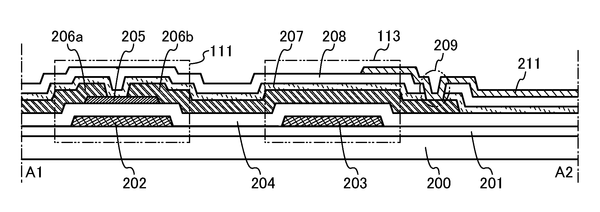
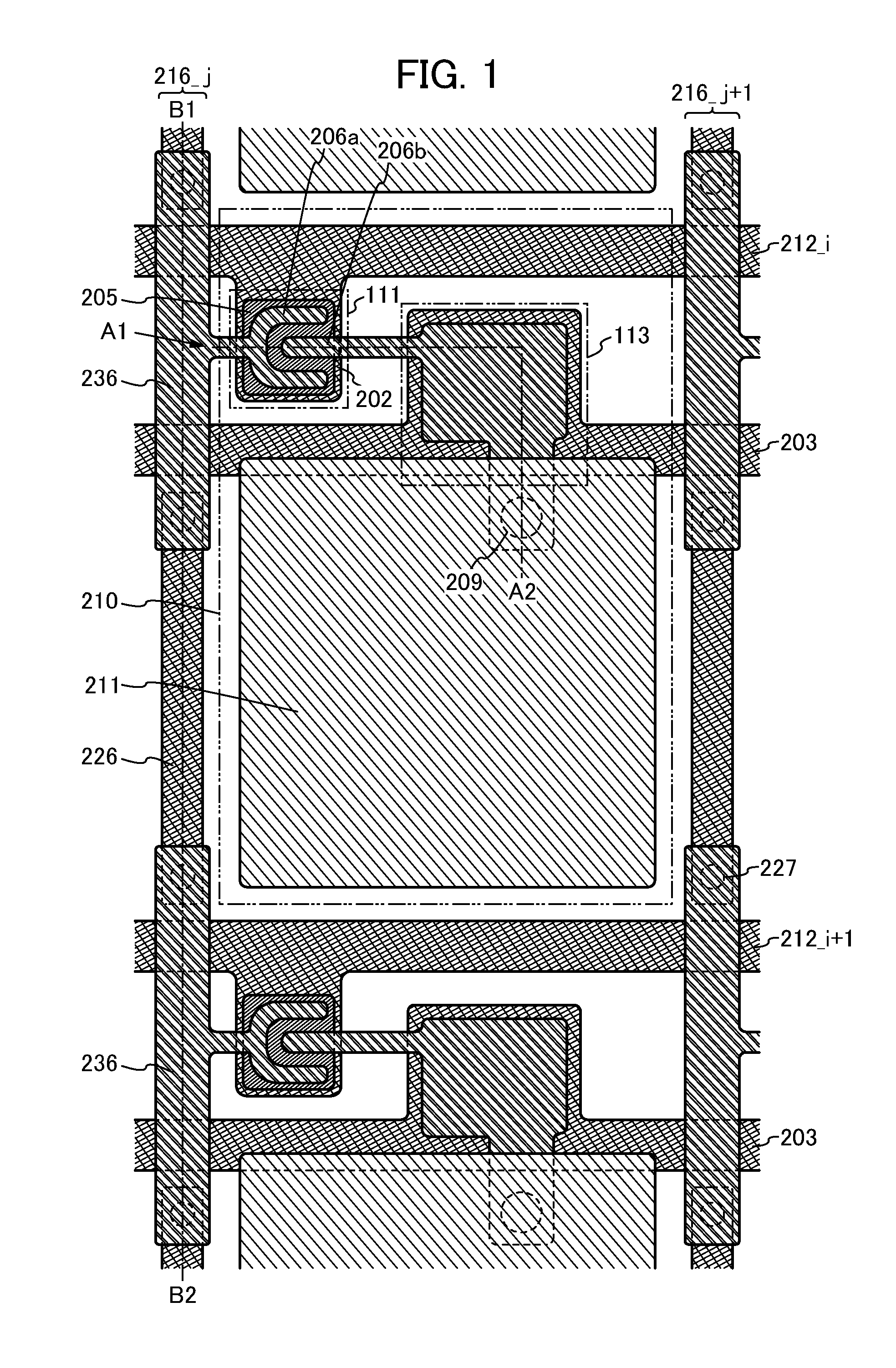
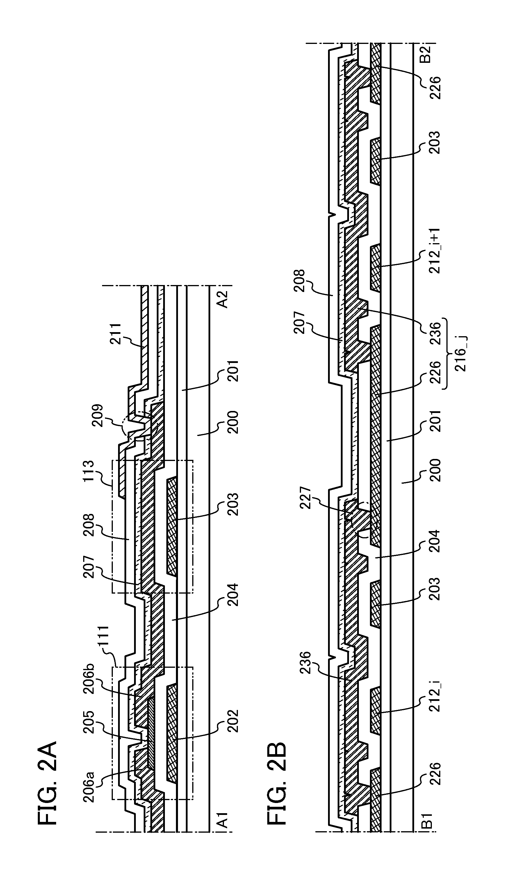
[0055]In this embodiment, examples of a configuration and a manufacturing method of a semiconductor device in which wiring resistance is reduced are described with reference toFIG. 1, FIGS. 2A and 2B, FIG. 3, FIG. 4, FIGS. 5A to 5C, FIG. 6, FIG. 7, FIGS. 8A and 8B, FIG. 9, FIGS. 10A1, 10A2, 10B1, and 10B2, FIGS. 11A1, 11A2, 11B1, 11B2, 11C1, 11C2, 11D1, and 11D2, FIGS. 12A1, 12A2, 12B1, and 12B2, FIGS. 13A1, 13A2, 13B1, 13B2, 13C1, and 13C2, FIGS. 14A to 14D, and FIGS. 15A to 15C. Note that in this embodiment, examples of application to a display device which is an embodiment of a semiconductor device are described.

[0056]FIG. 5A illustrates an example of the configuration of a semiconductor device 100 that can be used in a display device. The semiconductor device 100 includes a pixel region 102, a terminal portion 103 including m terminals 105 (m is an integer of greater than or equal to 1) and a terminal 107, and a terminal portion 104 including n terminals 106 (n is an integer of ...

embodiment 2

[0234]In this embodiment, examples of the display device described in the above embodiment are described with reference to FIGS. 16A to 16C and FIGS. 17A and 17B. Moreover, some or all of driver circuits which include the transistor an example of which is described in the above embodiment can be formed over a substrate where a pixel portion is formed, whereby a system-on-panel can be obtained.

[0235]In FIG. 16A, a sealant 4005 is provided to surround a pixel portion 4002 provided over a first substrate 4001, and the pixel portion 4002 is sealed using a second substrate 4006. In FIG. 16A, a signal line driver circuit 4003 and a scan line driver circuit 4004 each are formed using a single-crystal semiconductor or a polycrystalline semiconductor over a substrate prepared separately, and mounted in a region different from the region surrounded by the sealant 4005 over the first substrate 4001. Further, a variety of signals and potentials are supplied to the signal line driver circuit 400...

embodiment 3

[0282]In this embodiment, a semiconductor device having an image sensor function for reading data of an object is described as an example of the semiconductor device with reduced wiring resistance which is described in any of the above embodiments.

[0283]FIG. 18A shows an example of a semiconductor device having an image sensor function. FIG. 18A is an equivalent circuit of a photo sensor and FIG. 18B is a cross-sectional view showing part of the photo sensor.

[0284]One electrode of a photodiode 602 is electrically connected to a photodiode reset signal line 658, and the other electrode of the photodiode 602 is electrically connected to a gate of a transistor 640. One of a source and a drain of the transistor 640 is electrically connected to a photo sensor reference signal line 672, and the other of the source and the drain of the transistor 640 is electrically connected to one of a source and a drain of a transistor 656. A gate of the transistor 656 is electrically connected to a gat...


PUM


Abstract

To provide a semiconductor device with low power consumption in which a malfunction due to drop in voltage, delay of signal transmission, distortion of a signal waveform, and the like, which are caused by increase in wiring resistance, and decrease in reliability are prevented. A gate wiring is formed of a conductive layer containing copper, and a signal wiring formed of part of the same conductive layer as a source electrode and a drain electrode and a wiring formed of part of the same conductive layer as the gate wiring are electrically connected to each other in series or in parallel; thus, wiring resistance of the signal wiring is substantially decreased without an increase in width or thickness of the signal wiring.

Description

BACKGROUND OF THE INVENTION[0001]1. Field of the Invention[0002]The present invention relates to a semiconductor device and a manufacturing method thereof.[0003]In this specification and the like, the semiconductor device refers to any device which can function by utilizing semiconductor characteristics; an electro-optical device, a display device, a semiconductor circuit, and an electronic device are all included in the category of the semiconductor device.[0004]2. Description of the Related Art[0005]A technique by which a transistor (also referred to as a thin film transistor (TFT)) is formed using a semiconductor thin film formed over a substrate having an insulating surface has been attracting attention. The transistor has been applied to a wide range of electronic devices such as an integrated circuit (IC) and an image display device (display device). A silicon-based semiconductor material is widely known as a material for a semiconductor thin film applicable to a transistor. I...

Claims


Application Information

Patent Timeline
IPC IPC(8): H01L29/786
CPCH01L29/458H01L29/4908H01L29/78609H01L27/124H01L27/1225H01L27/1244H01L29/45H01L29/7869
Inventor YAMAZAKI, SHUNPEIKOYAMA, JUN
Owner SEMICON ENERGY LAB CO LTD
Learn More