
Semiconductor device

Inactive Publication Date: 2012-01-05
SEMICON ENERGY LAB CO LTD
View PDF7 Cites 9 Cited by
  • Summary
  • Abstract
  • Description
  • Claims
  • Application Information

AI Technical Summary

Benefits of technology

[0008]In view of the above problem, an object is to provide a semiconductor device including an oxide semiconductor, which has stable electric characteristics and high reliability.
[0024]According to one embodiment of the present invention, a semiconductor device including an oxide semiconductor, having favorable electric characteristics and high reliability can be provided.

Problems solved by technology

However, the electric conductivity of an oxide semiconductor might change when deviation from the stoichiometric composition due to deficiency of oxygen or the like occurs, or hydrogen or water forming an electron donor enters the oxide semiconductor during a manufacturing process of a device.

Method used


Image

  • Semiconductor device
  • Semiconductor device
  • Semiconductor device

Examples


embodiment 1

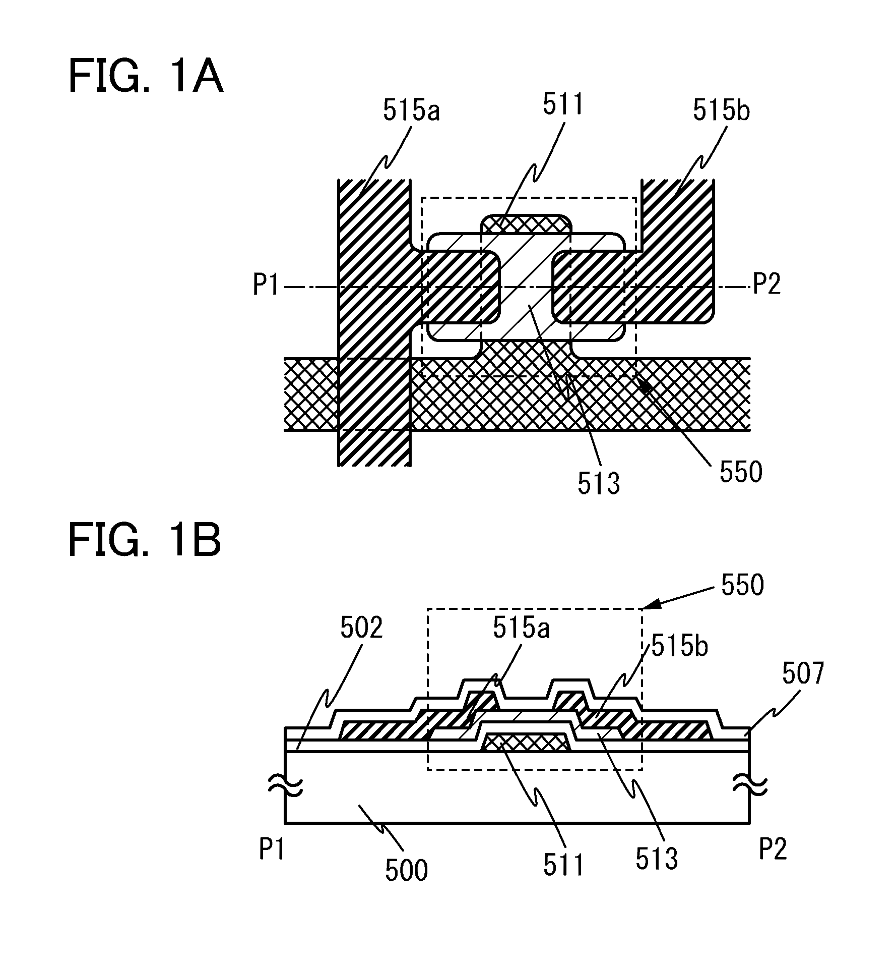
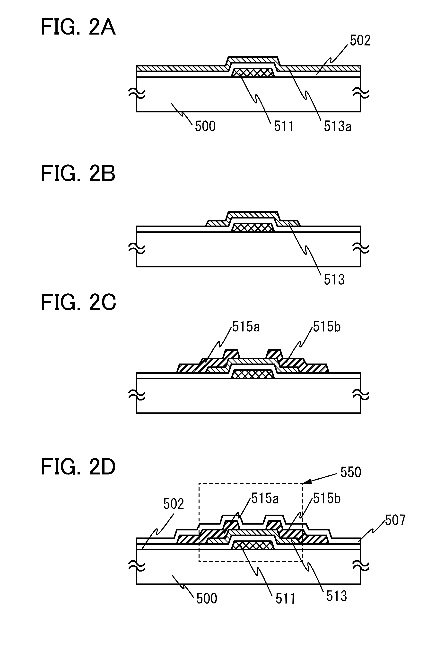
[0039]In this embodiment, a structure and a manufacturing method of a semiconductor device according to one embodiment of the present invention will be described with reference to FIGS. 1A and 1B, FIGS. 2A to 2D, FIGS. 3A and 3B, and FIG. 4.

[0040]FIGS. 1A and 1B illustrate a transistor 550 as an example of a semiconductor device. FIG. 1A is a top view of the transistor 550 and FIG. 1B is a cross-sectional view of the transistor 550. FIG. 1B illustrates a cross section along line P1-P2 in FIG. 1A.

[0041]In the transistor 550, a first gate electrode 511 and a gate insulating layer 502 which covers the first gate electrode 511 are provided over a substrate 500 having an insulating surface. An oxide semiconductor layer 513 which overlaps with the first gate electrode 511 is provided over the gate insulating layer 502. In addition, a first electrode 515a and a second electrode 515b which function as a source and a drain electrode are provided in contact with the oxide semiconductor layer ...

embodiment 2

[0105]A semiconductor device (also referred to as a display device) with a display function can be manufactured using the transistor an example of which is described in Embodiment 1. Moreover, some or all of the driver circuits which include the transistors can be formed over a substrate where the pixel portion is formed, whereby a system-on-panel can be obtained.

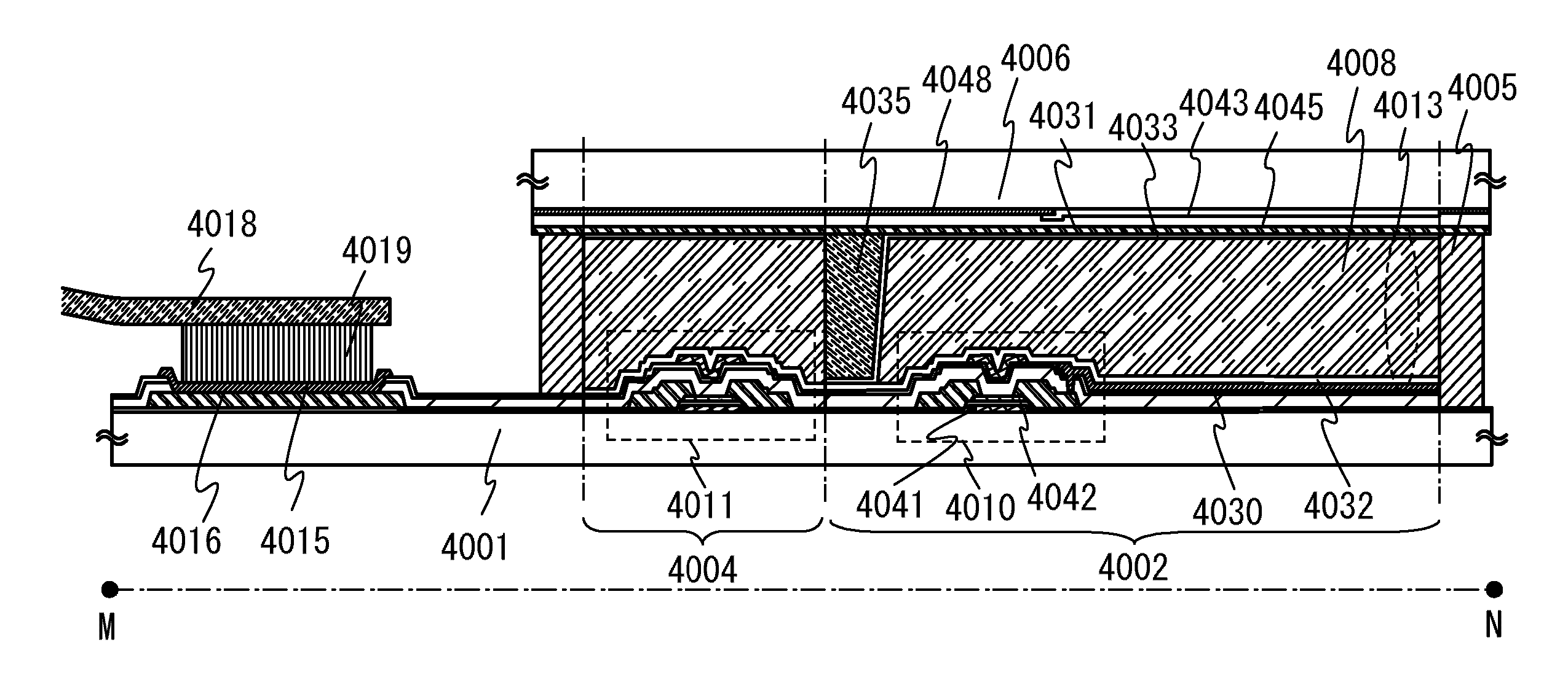
[0106]In FIG. 5A, a sealant 4005 is provided so as to surround a pixel portion 4002 provided over a first substrate 4001, and the pixel portion 4002 is sealed between the first substrate 4001 and the second substrate 4006. In FIG. 5A, a signal line driver circuit 4003 and a scan line driver circuit 4004 which are formed using a single crystal semiconductor film or a polycrystalline semiconductor film over a substrate separately prepared are mounted in a region that is different from the region surrounded by the sealant 4005 over the first substrate 4001. Various signals and potential are supplied to the signal line driver c...

embodiment 3

[0163]A semiconductor device disclosed in this specification can be applied to a variety of electronic devices (including game machines). Examples of electronic devices are a television set (also referred to as a television or a television receiver), a monitor of a computer or the like, a camera such as a digital camera or a digital video camera, a digital photo frame, a mobile phone handset (also referred to as a mobile phone or a mobile phone device), a portable game machine, a portable information terminal, an audio reproducing device, a large-sized game machine such as a pachinko machine, and the like. Examples of electronic devices each including the liquid crystal display device described in the above embodiment are described.

[0164]FIG. 9A is a laptop personal computer, which includes a main body 3001, a housing 3002, a display portion 3003, a keyboard 3004, and the like. By applying the semiconductor device of one embodiment of the present invention, the laptop personal compu...


PUM


Abstract

It is an object to provide a semiconductor device including an oxide semiconductor, which has stable electric characteristics and high reliability. A semiconductor device having a stacked-layer structure of a gate insulating layer; a first gate electrode in contact with one surface of the gate insulating layer; an oxide semiconductor layer in contact with the other surface of the gate insulating layer and overlapping with the first gate electrode; and a source electrode, a drain electrode, and an oxide insulating layer which are in contact with the oxide semiconductor layer is provided, in which the nitrogen concentration of the oxide semiconductor layer is 2×10¹⁹ atoms / cm3 or lower and the source electrode and the drain electrode include one or more of tungsten, platinum, and molybdenum.

Description

BACKGROUND OF THE INVENTION[0001]1. Field of the Invention[0002]The present invention relates to a semiconductor device including an oxide semiconductor. The present invention also relates to a manufacturing method of the semiconductor device. Note that semiconductor devices herein refer to general elements and devices which function by utilizing semiconductor characteristics.[0003]2. Description of the Related Art[0004]A technique by which transistors are formed using semiconductor thin films formed over a substrate having an insulating surface has been attracting attention. The transistor is applied to a wide range of electronic devices such as an integrated circuit (IC) or an image display device (display device). A silicon-based semiconductor material is widely known as a material for a semiconductor thin film applicable to a transistor. As another material, an oxide semiconductor has been attracting attention.[0005]For example, a transistor whose active layer includes an amorph...

Claims


Application Information

Patent Timeline
IPC IPC(8): H01L29/786
CPCH01L29/45H01L29/7869H01L29/78606H01L29/4908H01L29/78648H01L29/78693H01L29/517
Inventor YAMAZAKI, SHUNPEITAKAHASHI, MASAHIROHIROHASHI, TAKUYATOCHIBAYASHI, KATSUAKINAKAZAWA, YASUTAKAYOKOYAMA, MASATOSHI
Owner SEMICON ENERGY LAB CO LTD
Learn More