This helps you quickly interpret patents by identifying the three key elements:
Problems solved by technology
Method used
Benefits of technology
Benefits of technology
[0011]Glass substrates can be larger and can be obtained at lower cost than silicon wafers. Thus, by using a glass substrate as a supporting substrate, a large-area SOI substrate can be manufactured at low cost. However, the strain point of the glass substrate is equal to or lower than 700° C., and thus the glass substrate has low heat resistance. Therefore, the glass substrate cannot be heated at a temperature which exceeds the strain point of the glass substrate, and the process temperature is limited to 700° C. or lower. That is, there is a limitation on a process temperature in a step of reducing a crystal defect at a cleavage plane and a step of planarizing a surface.
[0014]In this manner, when a substrate such as a glass substrate, which has low heat resistance and is easily bent, is used for a supporting substrate, there is a problem in that it is difficult to reduce surface unevenness of a semiconductor layer that is separated from a silicon wafer so that the semiconductor layer is fixed to a supporting substrate.
[0025]By employing the present invention, a high-performance semiconductor device with favorable electric characteristics can be manufactured. Even when a semiconductor substrate which includes a single crystal semiconductor layer fixed to a supporting substrate having low heat resistance is used, the high-performance semiconductor device can be manufactured.
Problems solved by technology
However, the strain point of the glass substrate is equal to or lower than 700° C., and thus the glass substrate has low heat resistance.
Therefore, the glass substrate cannot be heated at a temperature which exceeds the strain point of the glass substrate, and the process temperature is limited to 700° C. or lower.
That is, there is a limitation on a process temperature in a step of reducing a crystal defect at a cleavage plane and a step of planarizing a surface.
In a conventional manner, a crystal defect of a single crystal semiconductor layer formed using a siliconwafer can be reduced by heating at a temperature of 1000° C. or higher; however, such a high-temperature process cannot be utilized for reducing a crystal defect of a single crystal semiconductor layer that is formed using a glass substrate having a strain point of 700° C. or lower.
In particular, it is difficult to perform mechanical polishing on a large-area glass substrate having a side that is longer than 30 cm.
Therefore, if there is large unevenness of the semiconductor layer, it is difficult to form a thin gate insulating layer with high withstand voltage.
Furthermore, large unevenness on the surface of the semiconductor layer leads to an increase of interface state density with the gate insulating layer or the like, which causes a degradation of electric characteristics of semiconductor elements such as a decrease in carrier mobility or an increase in threshold voltage.
In this manner, when a substrate such as a glass substrate, which has low heat resistance and is easily bent, is used for a supporting substrate, there is a problem in that it is difficult to reduce surface unevenness of a semiconductor layer that is separated from a siliconwafer so that the semiconductor layer is fixed to a supporting substrate.
Method used
Image
Click on the blue label to locate the original text in one second.
Reading with bidirectional positioning of images and text.
Examples
embodiment mode 1
[0059]In Embodiment Mode 1, a manufacturing method of a semiconductor device which uses a semiconductor substrate in which a single crystal semiconductor layer is fixed to a supporting substrate with a buffer layer interposed therebetween, will be described.
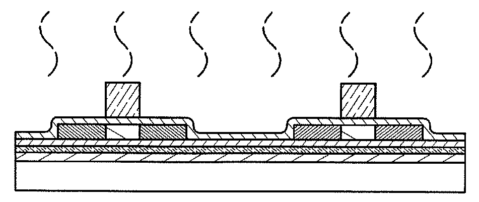
[0060]First, a method of forming a single crystal semiconductor layer over a supporting substrate will be described.
[0061]A single crystal semiconductor substrate 112 in which a separation layer 110 is formed in a region at a predetermined depth and a supporting substrate 102 are attached with a buffer layer 104 interposed therebetween so as to be bonded to each other (see FIG. 1A).
[0062]As the single crystal semiconductor substrate 112, a semiconductor substrate of silicon, germanium, or the like, a compound semiconductor substrate of galliumarsenide, indiumphosphide, or the like, or the like can be used. As for a single crystal silicon substrate which is a typical example of the single crystal semiconductor substrate, circula...
embodiment mode 2
[0195]In Embodiment Mode 2, a semiconductor substrate having another structure, which can be used for manufacture of a semiconductor device according to the present invention, will be described.
[0196]FIG. 16A illustrates an example in which the buffer layer 104 is formed on the supporting substrate 102. Between the single crystal semiconductor layer 120 and the supporting substrate 102, the insulating layer 106, an insulating layer 154, and an insulating layer 152 are formed from the single crystal semiconductor layer 120, and the stacked structure of these layers forms the buffer layer 104.
[0197]The insulating layer 152 may be an insulating layer similar to the insulating layer 107 and preferably includes at least one layer of insulating layer containing nitrogen. For example, at least one layer of insulating layer containing nitrogen as its composition such as a silicon nitride layer, a silicon nitrideoxide layer, or an aluminum nitride layer is formed. When the insulating layer ...
embodiment mode 3
[0203]In Embodiment Mode 3, transistors having a different structure from the above embodiment mode and a manufacturing method thereof will be described. Hereinafter, description is made with reference to the cross sectional views of FIGS. 4A to 4E, FIGS. 5A to 5D, and FIGS. 6A to 6C. Note that a method of manufacturing an n-channel transistor and a p-channel transistor at the same time will be described in this embodiment mode.
[0204]First, as illustrated in FIG. 4A, a semiconductor substrate is prepared. In this embodiment mode, the semiconductor substrate manufactured through the steps of FIGS. 1A to 1E in Embodiment Mode 1 is used. In other words, the semiconductor substrate in which the single crystal semiconductor layer 120 is fixed over the supporting substrate 102 with the buffer layer 104 interposed therebetween is used. The single crystal semiconductor layer 120 is a semiconductor layer part of which is re-single-crystallized through melting by laser beam irradiation. Note ...
PUM
Abstract
A single crystalsemiconductor substrate bonded over a supporting substrate with a buffer layer interposed therebetween and having a separation layer is heated to separate the single crystalsemiconductor substrate using the separation layer or a region near the separation layer as a separation plane, thereby forming a single crystalsemiconductor layer over the supporting substrate. The single crystal semiconductor layer is irradiated with a laser beam to re-single-crystallize the single crystal semiconductor layer through melting. An impurity element is selectively added into the single crystal semiconductor layer to form a pair of impurity regions and a channel formation region between the pair of impurity regions. The single crystal semiconductor layer is heated at temperature which is equal to or higher than 400° C. and equal to or lower than a strain point of the supporting substrate and which does not cause melting of the single crystal semiconductor layer.
Description
BACKGROUND OF THE INVENTION[0001]1. Field of the Invention[0002]The present invention relates to a semiconductor device which is manufactured using a semiconductor substrate including a single crystal semiconductor layer formed over an insulating surface, and a manufacturing method thereof.[0003]Note that a semiconductor device in this specification refers to all types of devices which can function by utilizing semiconductor characteristics, and electro-optic devices (including EL display devices and liquid crystal display devices), semiconductor circuits, and electronic devices are all included in the category of the semiconductor device.[0004]2. Description of the Related Art[0005]With development of VLSI technology, lower power consumption and higher speed operation over the scaling law which can be realized by bulk single crystal silicon have been demanded. In order to improve such characteristics, an SOI (silicon on insulator) structure has been attracting attention these days....
Claims
Application Information
Patent Timeline
Application Date:The date an application was filed.
Publication Date:The date a patent or application was officially published.
First Publication Date:The earliest publication date of a patent with the same application number.
Issue Date:Publication date of the patent grant document.
PCT Entry Date:The Entry date of PCT National Phase.
Estimated Expiry Date:The statutory expiry date of a patent right according to the Patent Law, and it is the longest term of protection that the patent right can achieve without the termination of the patent right due to other reasons(Term extension factor has been taken into account ).
Invalid Date:Actual expiry date is based on effective date or publication date of legal transaction data of invalid patent.

