

Semiconductor Device and Method of Manufacturing the Same
- Summary
- Abstract
- Description
- Claims
- Application Information
AI Technical Summary
Benefits of technology
Problems solved by technology
Method used
Image

Examples
Embodiment Construction
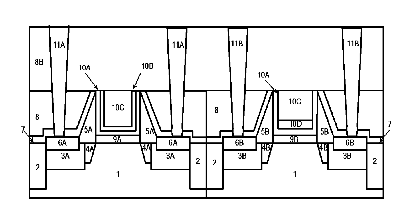
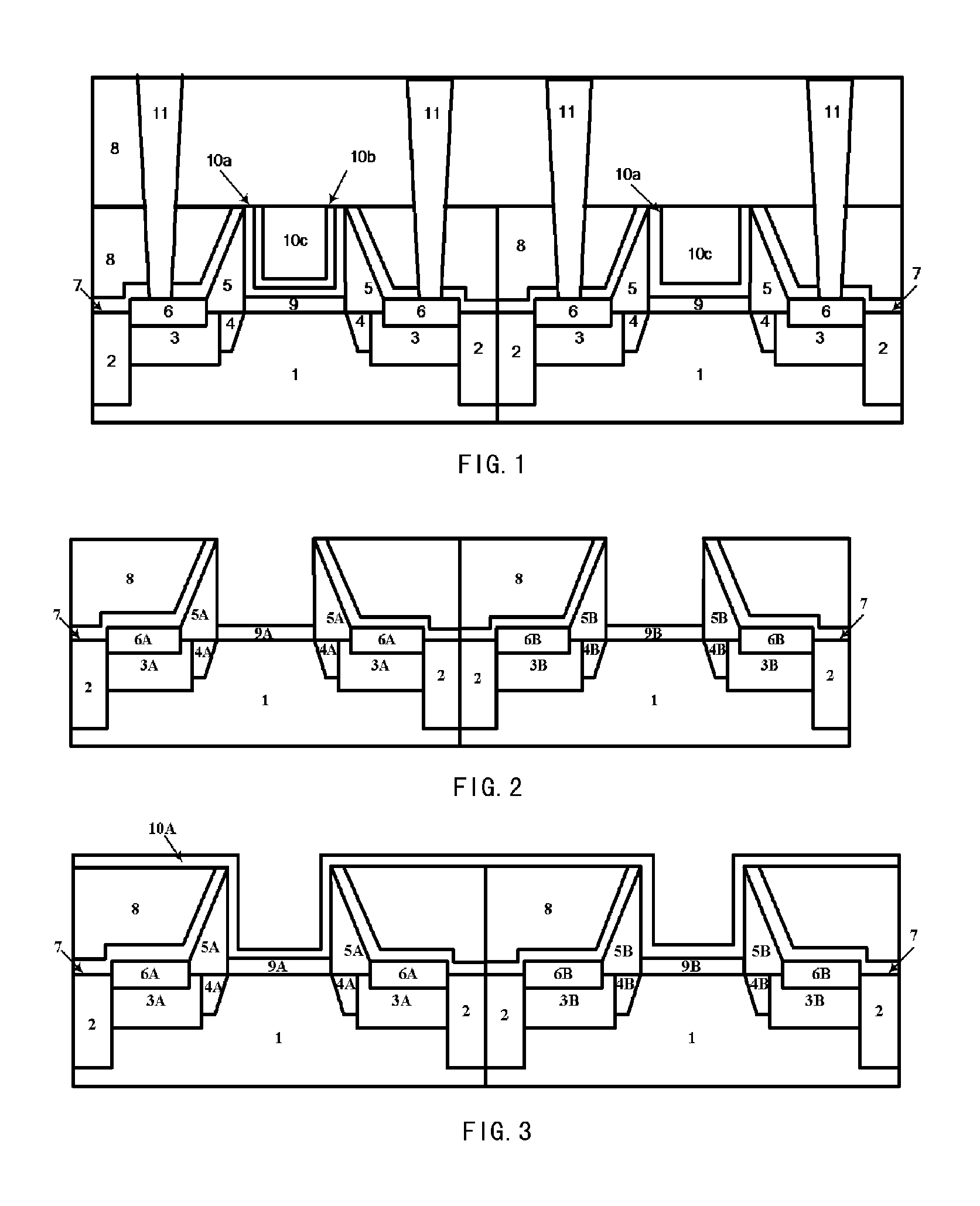
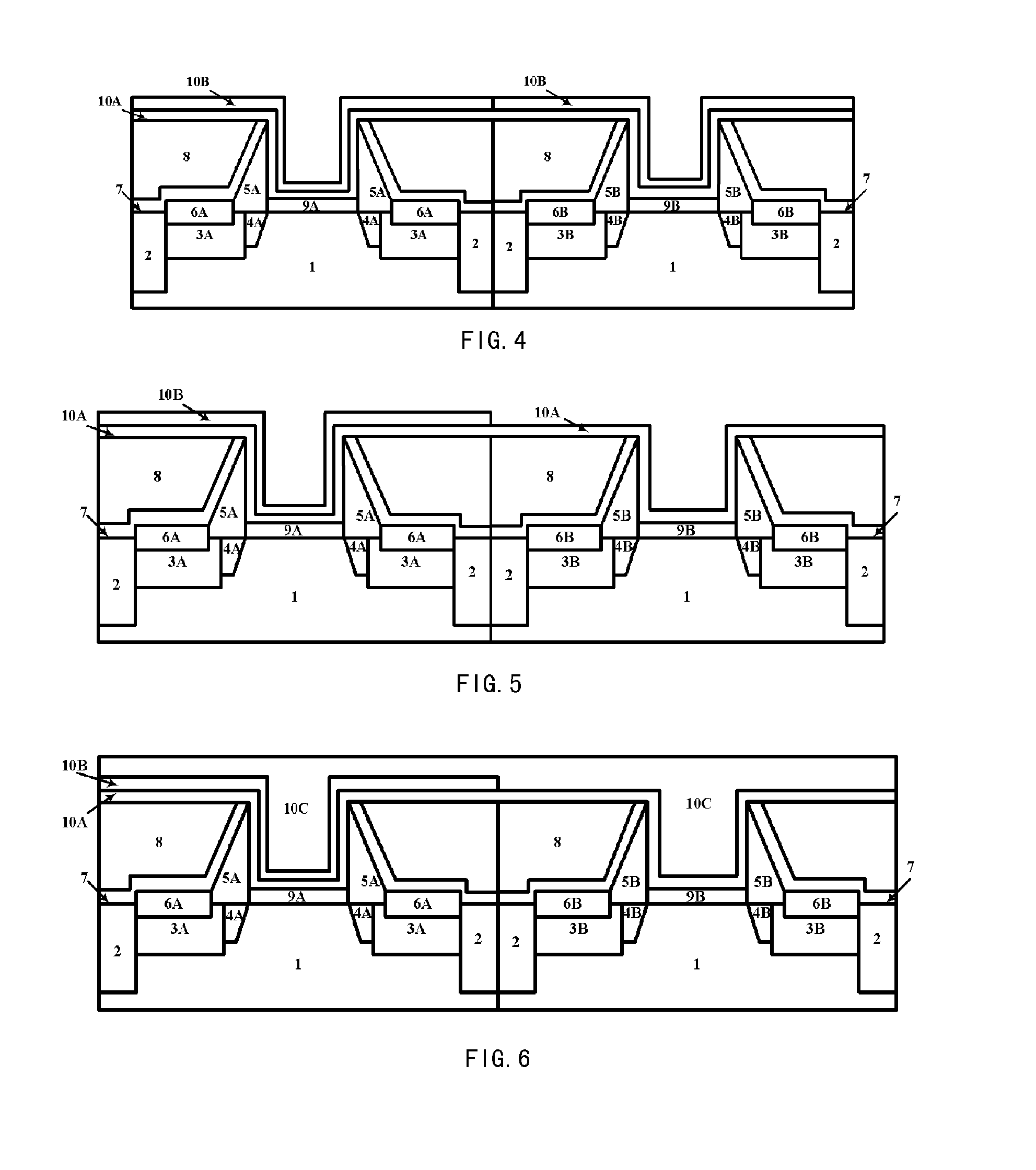
[0036]The features of the technical solutions of the present invention and the technical effects thereof are explained in detail in combination with the illustrative embodiments with reference to the drawings below, and a new type of CMOSFET capable of effectively regulating a metal gate work function to thereby control the threshold and a method of manufacturing the same are disclosed. It shall be noted that like reference signs indicate like structures, and the terms like “first”, “second”, “on” and “below” etc. used in the present application may be used to modify various device structures or manufacturing processes. Unless specific explanations, such modifications do not imply the spatial, sequential or hierarchical relationships of the device structures or manufacturing processes.
[0037]The steps of the method for manufacturing a MOSFET in accordance with the present invention will be described in detail with reference to the diagrammatic cross-sections in FIGS. 2-10, wherein, p...
PUM
 Abstract
Description
Claims
Application Information