
Dielectric composition and multilayer ceramic electronic component including the same

Active Publication Date: 2013-09-26
SAMSUNG ELECTRO MECHANICS CO LTD
View PDF0 Cites 12 Cited by
  • Summary
  • Abstract
  • Description
  • Claims
  • Application Information

AI Technical Summary

Benefits of technology

This patent provides a dielectric material that has high dielectric constant and can withstand high temperatures without becoming too thin. This material is reliable and suitable for use in multilayer ceramic electronic components.

Problems solved by technology

Heat generated by electronic devices is a growing problem, since the average size of image display devices has recently been enlarged, while the rates of central processing units (CPUs) included in computers have also increased.
However, when the multilayer ceramic capacitor is manufactured as above, in the case in which the dielectric layer is thinned and voltage is boosted, the strength of an electric field across the dielectric layers may be increased due to the boosting of voltage, which may degrade DC-bias characteristics and reliability.
Furthermore, the formation of thin layers may cause defects in layer microstructure, to thereby degrade high-temperature withstand voltage characteristics, such as breakdown voltage (BDV), insulation resistance (IR), and the like.
However, as particles of the base powder are reduced in size, the user-desired amount and temperature characteristics may be difficult to implement and the dielectric constant may be decreased.

Method used


Image

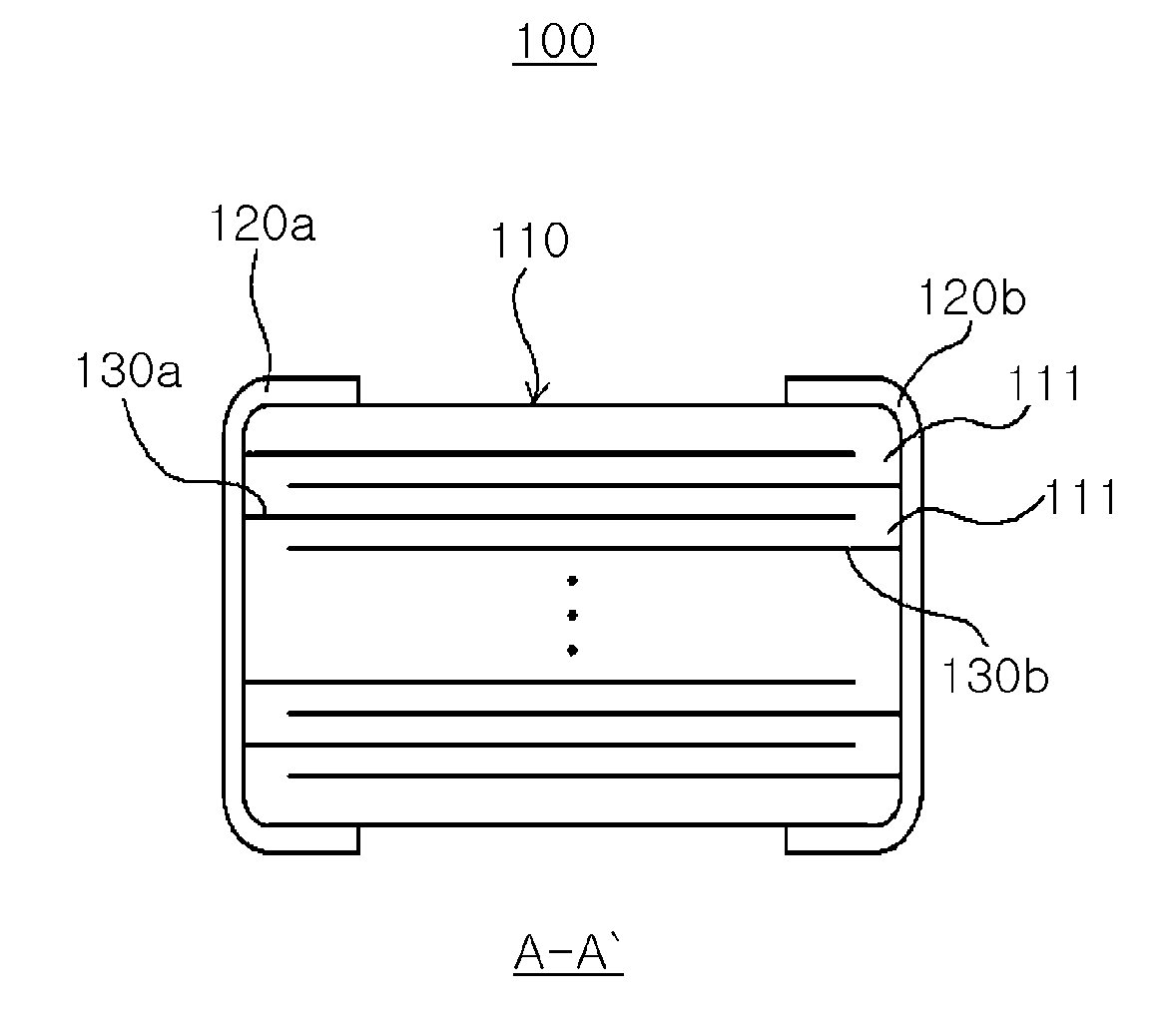
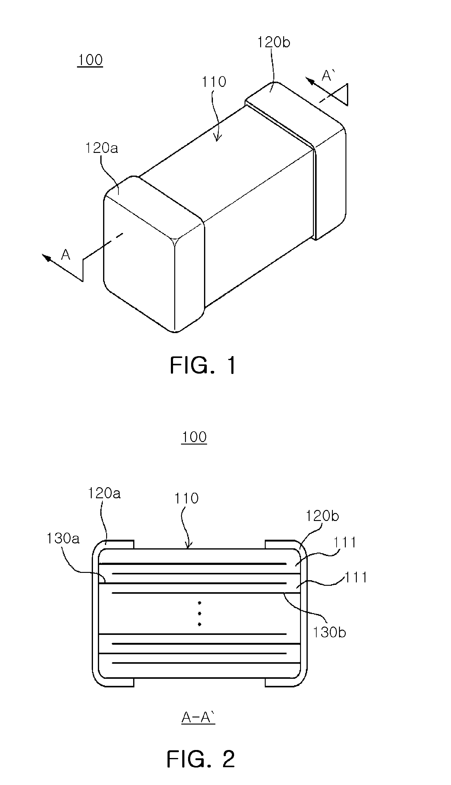
  • Dielectric composition and multilayer ceramic electronic component including the same
  • Dielectric composition and multilayer ceramic electronic component including the same
  • Dielectric composition and multilayer ceramic electronic component including the same

Examples


Embodiment Construction

[0035]Hereinafter, embodiments of the present invention will be described in detail with reference to the accompanying drawings.

[0036]However, the invention may be embodied in many different forms and should not be construed as being limited to the embodiments set forth herein.

[0037]The embodiments of the present invention are provided so that those skilled in the art may more completely understand the present invention.

[0038]In the drawings, the shapes and dimensions of components may be exaggerated for clarity, and the same reference numerals will be used throughout to designate the same or like components.

[0039]In addition, like reference numerals denote parts performing similar functions and actions throughout the drawings.

[0040]In addition, unless explicitly described otherwise, “comprising” any components will be understood to imply the inclusion of other components but not the exclusion of any other components.

[0041]The present invention is directed to a dielectric compositio...


PUM

PropertyMeasurementUnit
Thicknessaaaaaaaaaa
Substance countaaaaaaaaaa

Abstract

There is provided a dielectric composition, including: a base powder including BamTiO3, where 0.995≦m≦1.010; a first subcomponent including 0.1 to 1.0 at % (x) of an oxide or carbonate containing at least one variable-valence acceptor element based on 100 moles of the base powder; a second subcomponent including 0.01 to 3.0 at % (y) of an oxide or carbonate containing at least one fixed valence acceptor element; a third subcomponent including an oxide or carbonate containing cerium (z) at % and at least one other rare-earth element (w) at %, where 0.01≦z≦x+4y and 0.01≦z+w≦x+4y; a fourth subcomponent including at least one of an oxide or carbonate containing at least one of Barium, Calcium, Aluminum, and Silicon and glass containing silicon; and a fifth subcomponent including 0.01 to 10.0 at % of an oxide containing zirconium.

Description

CROSS-REFERENCE TO RELATED APPLICATIONS[0001]This application claims the priority of Korean Patent Application No. 10-2012-0028212 filed on Mar. 20, 2012, in the Korean Intellectual Property Office, the disclosure of which is incorporated herein by reference.BACKGROUND OF THE INVENTION[0002]1. Field of the Invention[0003]The present invention relates to a dielectric composition and a multilayer ceramic electronic component including the same.[0004]2. Description of the Related Art[0005]Examples of electronic components using a ceramic material include a capacitor, an inductor, a piezoelectric element, a varistor, a thermistor and the like.[0006]Among these ceramic electronic components, a multilayer ceramic capacitor (MLCC) has a small size, secures high capacitance, and is easily mountable.[0007]A multilayer ceramic capacitor is a chip type condenser that is mounted on circuit boards of several electronic products, for example, an image display device, such as a liquid crystal disp...

Claims


Application Information

Patent Timeline
IPC IPC(8): C04B35/468H01G4/008
CPCC04B35/468H01G4/1227C04B35/4682C04B2235/3206C04B2235/3208C04B2235/3215C04B2235/3217C04B2235/3224C04B2235/3225C04B2235/3229C04B2235/3236C04B2235/3239C04B2235/3241C04B2235/3244C04B2235/3262C04B2235/3267C04B2235/3272C04B2235/3275C04B2235/3279C04B2235/3281C04B2235/3284C04B2235/3418C04B2235/36C04B2235/442C04B2235/5445C04B2235/652C04B2235/6582C04B2235/663C04B2235/79H01G4/30H01G4/008C04B35/48C04B35/50H01B3/12
Inventor KIM, KYU REEYOON, SEOK HYUNYOON, SUN HOKIM, CHANG HOON
Owner SAMSUNG ELECTRO MECHANICS CO LTD
Learn More