

Low electron temperature, edge-density enhanced, surface wave plasma (SWP) processing method and apparatus
a surface wave plasma and electron temperature technology, applied in plasma technique, inductance/transformer/magnet manufacturing, waveguide type devices, etc., can solve the problems of still suffering the practical implementation of swp sources, and achieve enhanced plasma uniformity, low electron temperature, and high degree of ionization
- Summary
- Abstract
- Description
- Claims
- Application Information
AI Technical Summary
Benefits of technology
Problems solved by technology
Method used
Image

Examples
Embodiment Construction
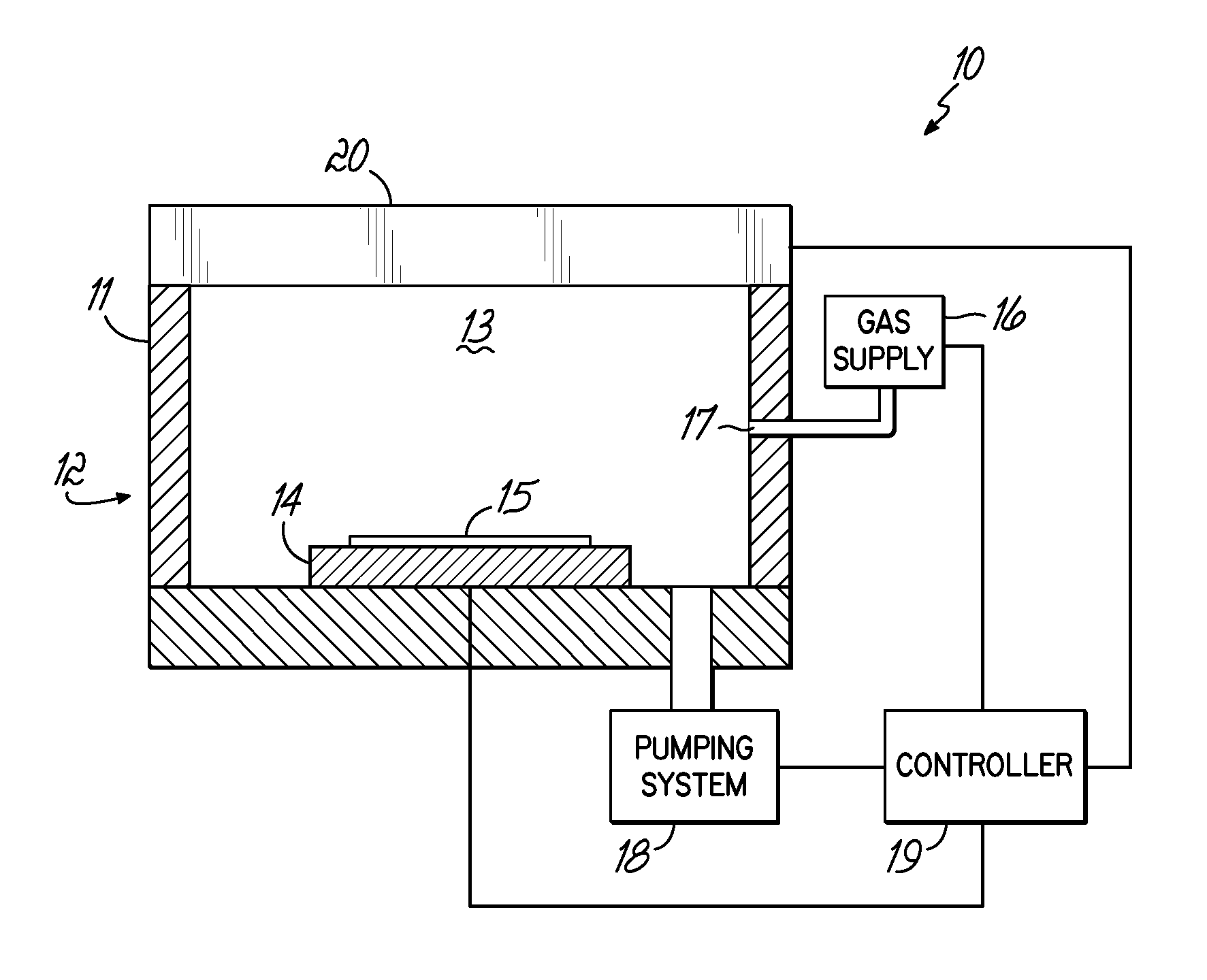
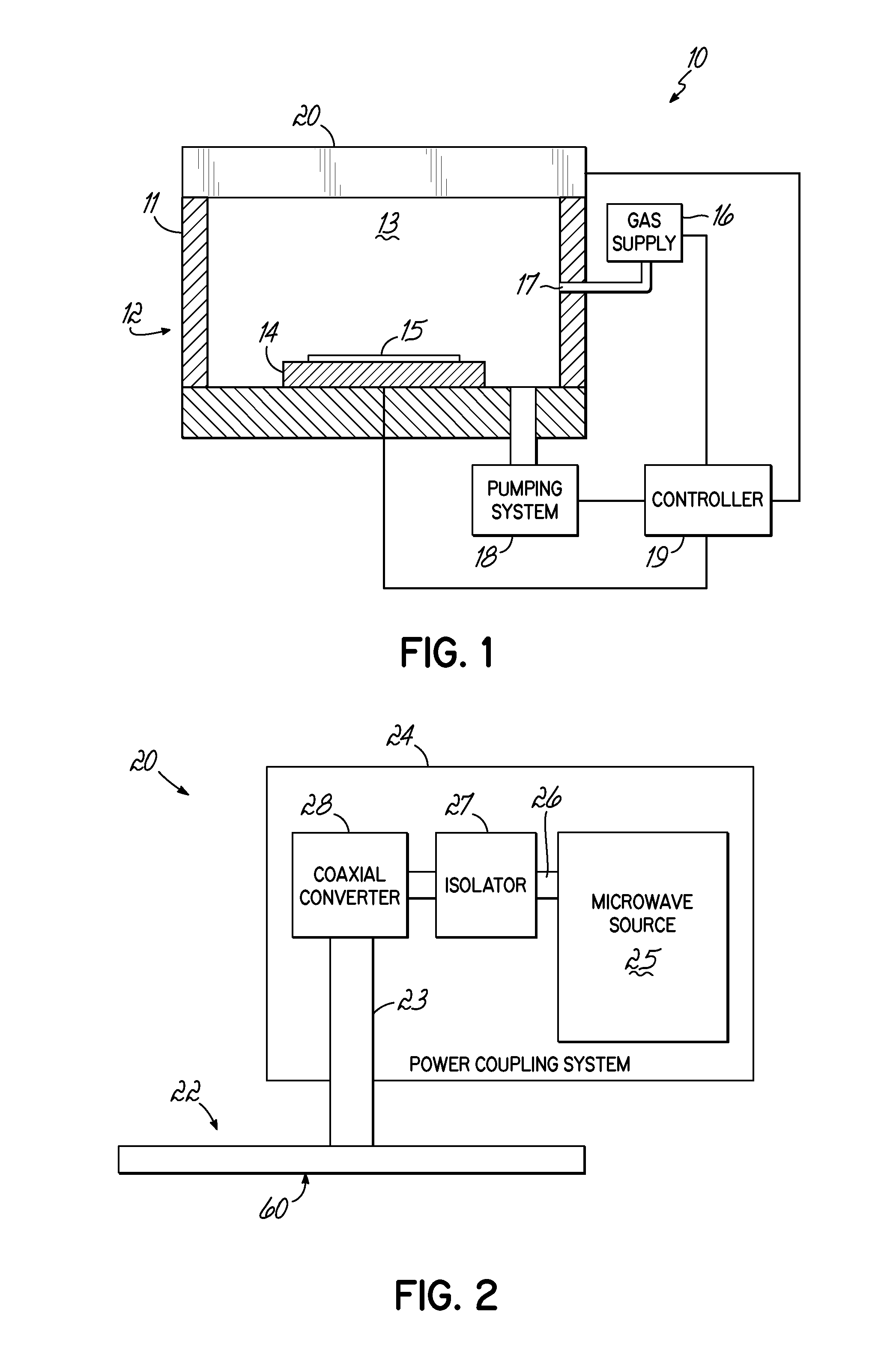
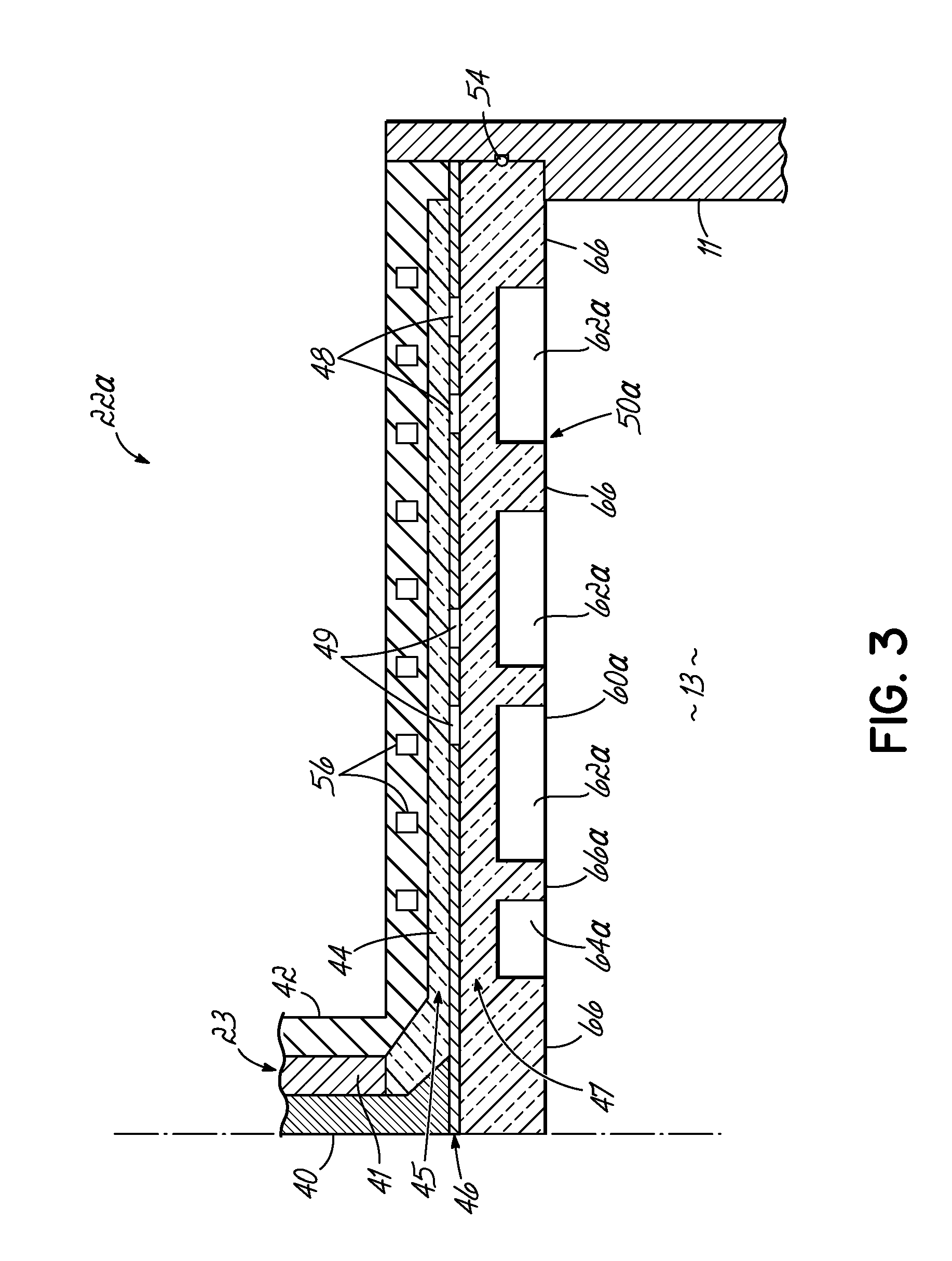
[0027]A microwave plasma processing method and apparatus are disclosed in various embodiments. However, one skilled in the relevant art will recognize that the various embodiments may be practiced without one or more of the specific details, or with alternative methods, materials, or components. Well-known structures, materials, or operations are not shown or described in detail to avoid obscuring aspects of various embodiments of the invention.
[0028]Similarly, for purposes of explanation, specific numbers, materials, and configurations are set forth in order to provide a thorough understanding of the invention. Nevertheless, the invention may be practiced with alternative specific details. Furthermore, the various embodiments shown in the figures are illustrative representations and are not necessarily drawn to scale.
[0029]References throughout this specification to “one embodiment” or “an embodiment” or “certain embodiments” or variations thereof means that a particular feature, s...
PUM
| Property | Measurement | Unit |
|---|---|---|
| diameter | aaaaa | aaaaa |
| power | aaaaa | aaaaa |
| power | aaaaa | aaaaa |
Abstract
Description
Claims
Application Information