Stratified gate dielectric stack for gate dielectric leakage reduction

Inactive Publication Date: 2013-10-24
IBM CORP
View PDF7 Cites 32 Cited by
  • Summary
  • Abstract
  • Description
  • Claims
  • Application Information

AI Technical Summary

Benefits of technology

[0005]The gate leakage can be reduced without impact to the effective work function of the gate stack by employing a dielectric material layer that disrupts the band gap of a high-k gate dielectric, providing benefits to field effect transistors of all polarities on a semiconductor substrate. The dielectric material layer that disrupts the band gap structure of a gate dielectric material can be inserted in the middle of the gate dielectric material to form a gate dielectric composed of a stratified gate dielectric stack. The stratified gate dielectric stack includes a first high dielectric constant (high-k) gate dielectric comprising a first high-k dielectric material, a band-gap-disrupting dielectric comprising a dielectric material having a different band gap than the first high-k dielectric material, and a second high-k gate dielectric comprising a second high-k dielectric material. The second high-k dielectric material can be the same as, or different from, the first high-k dielectric material. The band-gap-disrupting dielectric includes at least one contiguous atomic layer of the dielectric material. Thus, the stratified gate dielectric stack includes a first atomic interface between the first high-k gate dielectric and the band-gap-disrupting dielectric, and a second atomic interface between the second high-k gate dielectric and the band-gap-disrupting dielectric that is spaced from the first atomic interface by at least one continuous atomic layer

Problems solved by technology

One of the main challenges in advanced high-performance field effect transistors is the high gate leakage current through a high-k gate dielectric between the gate electrode and the body of a field effect transistor.
The high-

Method used


Image

  • Stratified gate dielectric stack for gate dielectric leakage reduction
  • Stratified gate dielectric stack for gate dielectric leakage reduction
  • Stratified gate dielectric stack for gate dielectric leakage reduction

Examples


first embodiment

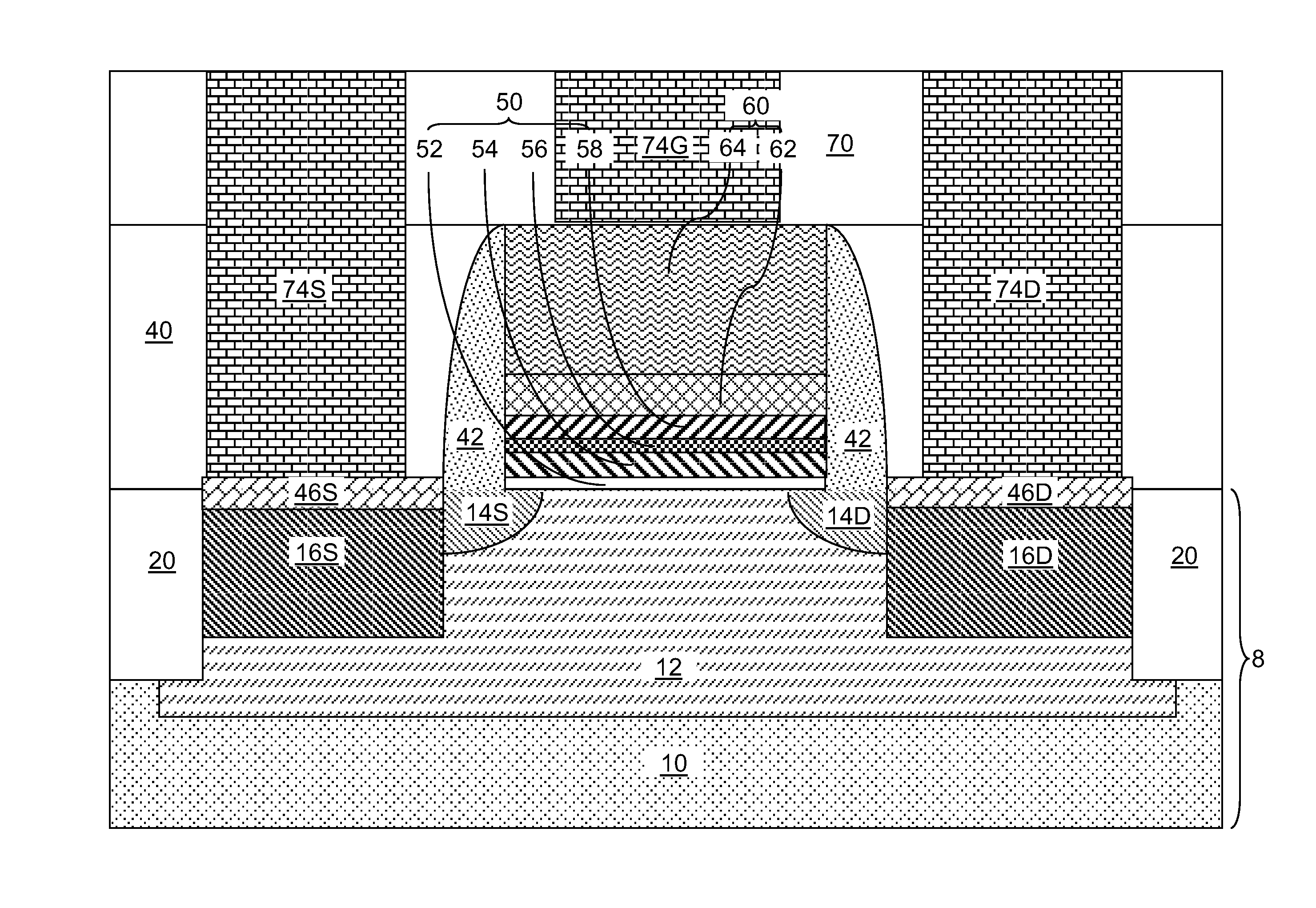
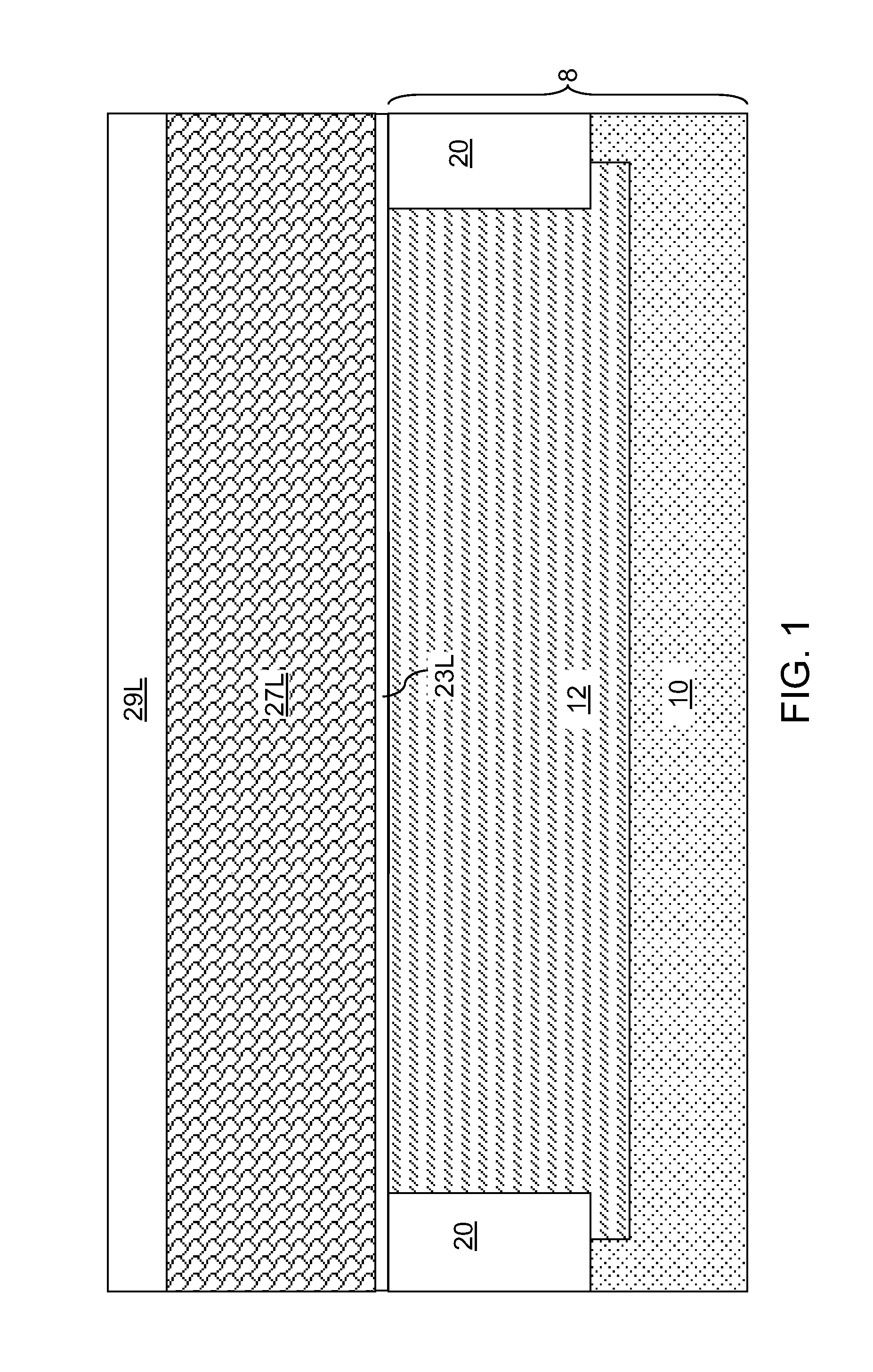
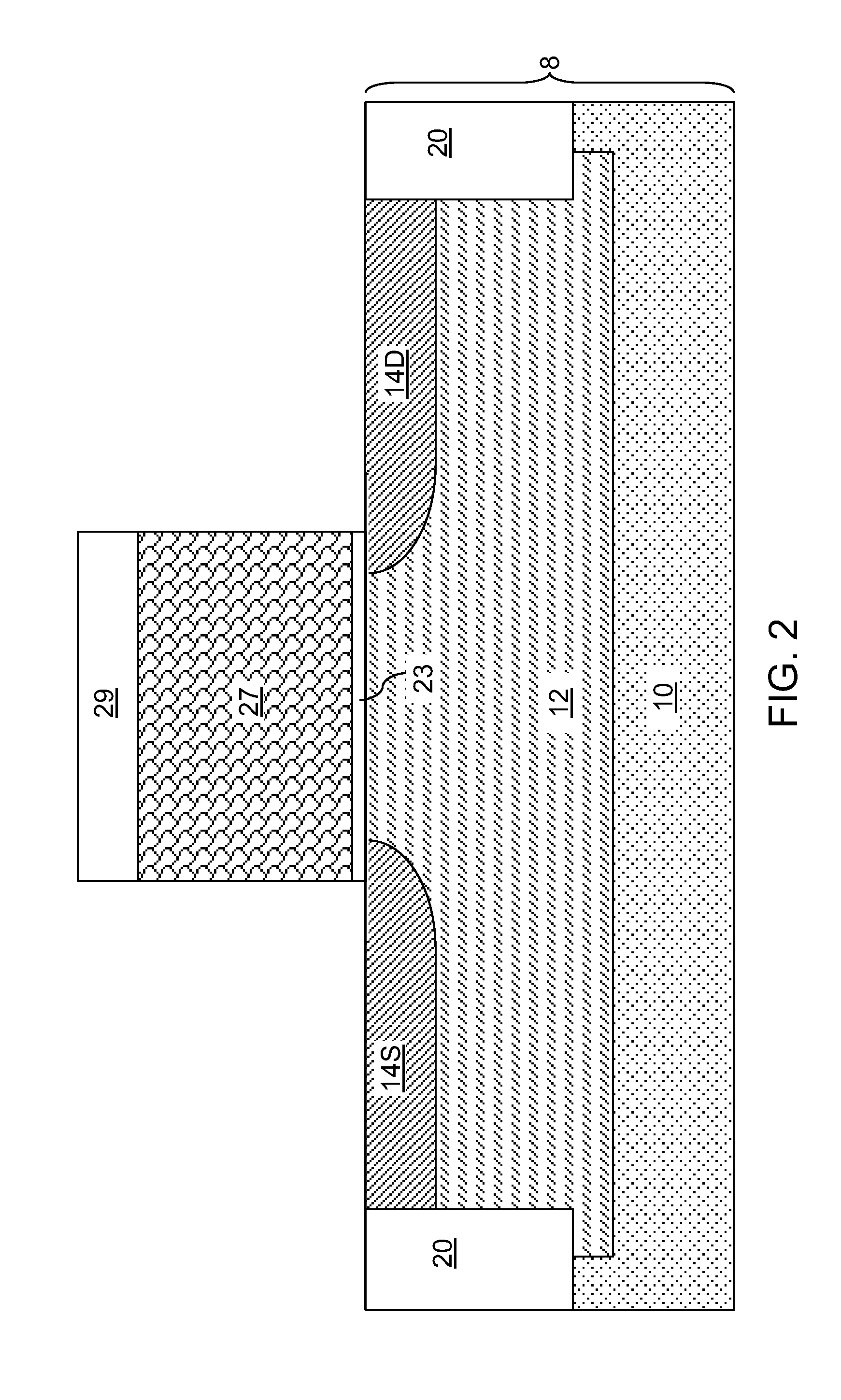
[0031]Referring to FIG. 1, a first exemplary semiconductor structure according to the present disclosure includes a semiconductor substrate 8, on which various components of field effect transistors are subsequently formed. The semiconductor substrate 8 can be a bulk substrate including a bulk semiconductor material throughout, or a semiconductor-on-insulator (SOI) substrate (not shown) containing a top semiconductor layer, a buried insulator layer located under the top semiconductor layer, and a bottom semiconductor layer located under the buried insulator layer.

[0032]Various portions of the semiconductor material in the semiconductor substrate 8 can be doped with electrical dopants of n-type or p-type at different dopant concentration levels. For example, the semiconductor substrate 8 may include an underlying semiconductor layer 10 and an active region 12 having a doping different from the doping of the underlying semiconductor layer 10. The active region 12 can be a doped well. ...

second embodiment

[0086]Referring to FIG. 13, a second exemplary semiconductor structure including a finFET having a gate dielectric 50 including a stratified gate dielectric stack is shown according to the present disclosure. A semiconductor-on-insulator (SOI) substrate including a handle substrate 110, a buried insulator layer 112, and a top semiconductor layer can be employed to form a semiconductor fin 9 on a substrate 8′ including the stack of the handle substrate 110 and the buried insulator layer 112. A body region 12′, a source extension region 14S, a drain extension region 14D can be formed within the semiconductor fin 9 prior to formation of a disposable gate structure straddling over the semiconductor fin 9. In the second exemplary semiconductor structure, the semiconductor fin 9 formed on a stack, from bottom to top, of a handle substrate 110 and a buried insulator layer 112 constitutes a semiconductor substrate.

[0087]The processing steps of FIGS. 1-7, one of 8 and 8A, 9-11, and one of 12...

third embodiment

[0090]Referring to FIG. 14, a third exemplary semiconductor structure according to the present disclosure is shown. In the third exemplary semiconductor structure, after formation of an interfacial dielectric layer, each of the first high-k gate dielectric layer 54L, the band-gap-disrupting dielectric layer 56L, the second high-k gate dielectric layer 58L, the work function material layer 62L, and the conductive material layer 64L, the work function material layer, and the conductive material layer 64L is deposited as planar layers below a temperature above which inter-atomic diffusion occurs at a detectable level across the first atomic interface or across the second atomic interface in lieu of deposition of the disposable gate level layers (23L, 27L, 29L) illustrated in FIG. 1. The temperature above which the inter-atomic diffusion occurs across the first atomic interface or across the second atomic interface is less than 800 degrees Celsius, and is typically in a range between 70...


PUM


Abstract

A stratified gate dielectric stack includes a first high dielectric constant (high-k) gate dielectric comprising a first high-k dielectric material, a band-gap-disrupting dielectric comprising a dielectric material having a different band gap than the first high-k dielectric material, and a second high-k gate dielectric comprising a second high-k dielectric material. The band-gap-disrupting dielectric includes at least one contiguous atomic layer of the dielectric material. Thus, the stratified gate dielectric stack includes a first atomic interface between the first high-k gate dielectric and the band-gap-disrupting dielectric, and a second atomic interface between the second high-k gate dielectric and the band-gap-disrupting dielectric that is spaced from the first atomic interface by at least one continuous atomic layer of the dielectric material of the band-gap-disrupting dielectric. The insertion of the band-gap disrupting dielectric results in lower gate leakage without resulting in any substantial changes in the threshold voltage characteristics and effective oxide thickness.

Description

CROSS REFERENCE TO RELATED APPLICATION[0001]This application is a continuation of U.S. patent application Ser. No. 13 / 449,647, filed Apr. 18, 2012 the entire content and disclosure of which is incorporated herein by reference.BACKGROUND[0002]The present disclosure generally relates to semiconductor devices, and particularly to a semiconductor structure having a gate dielectric comprising a stratified gate dielectric stack comprising two atomic interfaces that provide discontinuities in the band gap structure of the gate dielectric, and methods of manufacturing the same.[0003]One of the main challenges in advanced high-performance field effect transistors is the high gate leakage current through a high-k gate dielectric between the gate electrode and the body of a field effect transistor. The high-k gate dielectric consisting of a single homogeneous dielectric material requires to be continually reduced in thickness to obtain higher performance of the field effect transistor but at t...

Claims


Application Information

Patent Timeline
IPC IPC(8): H01L29/78H01L29/51
CPCH01L21/28211H01L29/518H01L29/66545H01L29/6659H01L29/7833H01L29/4958H01L29/513H01L21/28158H01L21/283H01L29/6656H01L29/66795H01L21/28202H01L29/4966H01L29/785
Inventor JAGANNATHAN, HEMANTHJAMISON, PAUL C.
Owner IBM CORP
Why Eureka
Try Eureka