Method of driving semiconductor device
a technology of semiconductor devices and semiconductor devices, which is applied in the direction of logic circuits, pulse techniques, and reliability increasing modifications, can solve the problems of large change in the potential supplied to the switching transistor, large change in the potential of the gate electrode, etc., and achieve the effect of reducing the power consumption of the semiconductor devi
- Summary
- Abstract
- Description
- Claims
- Application Information
AI Technical Summary
Benefits of technology
Problems solved by technology
Method used
Image

Examples
embodiment 1
[0047]In this embodiment, a semiconductor device and a method of driving the semiconductor device according to one embodiment of the present invention are described with reference to drawings.
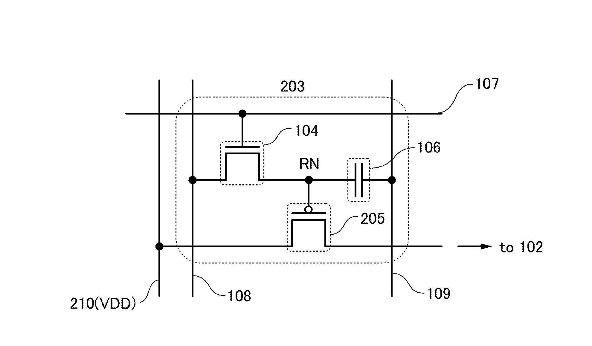
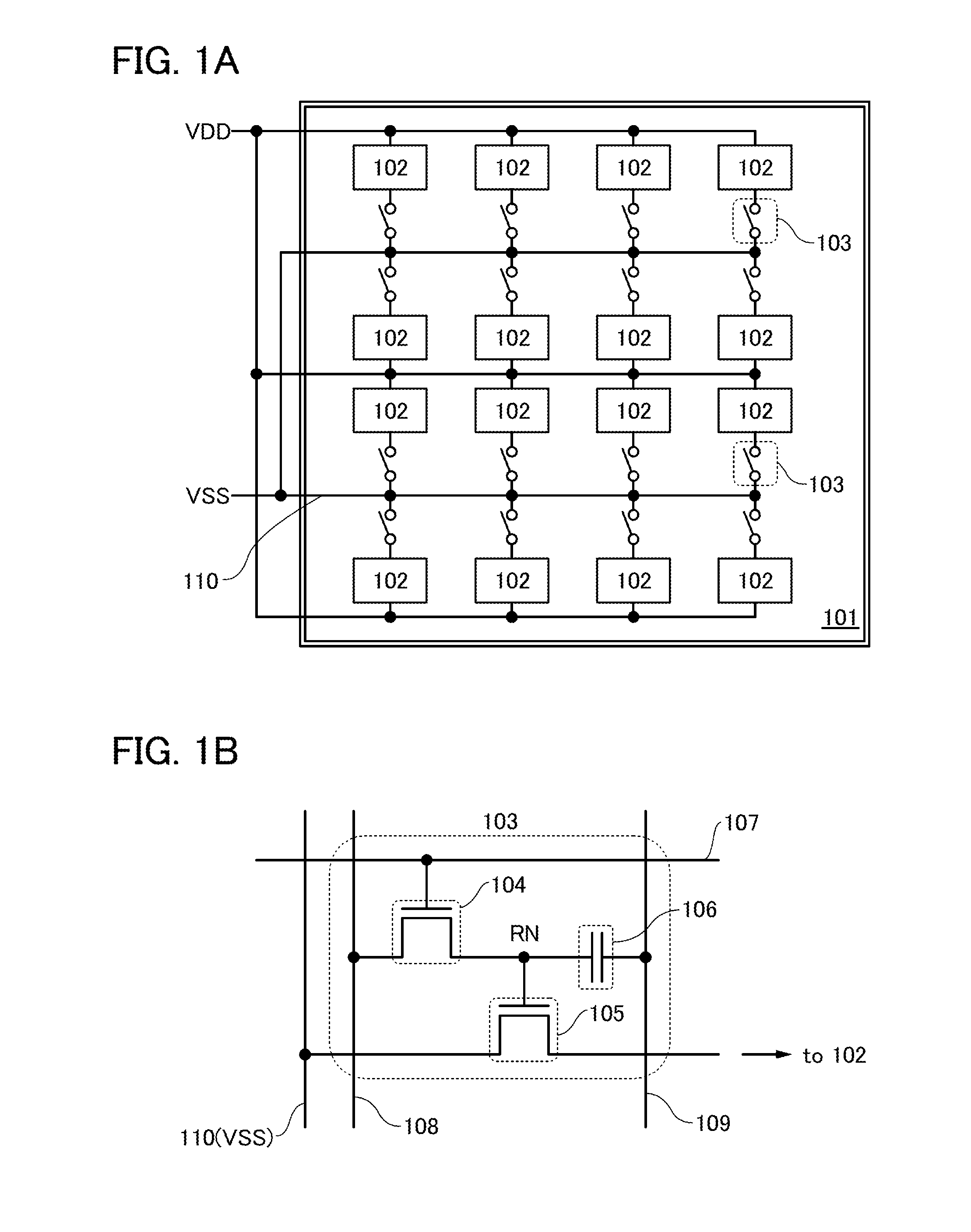
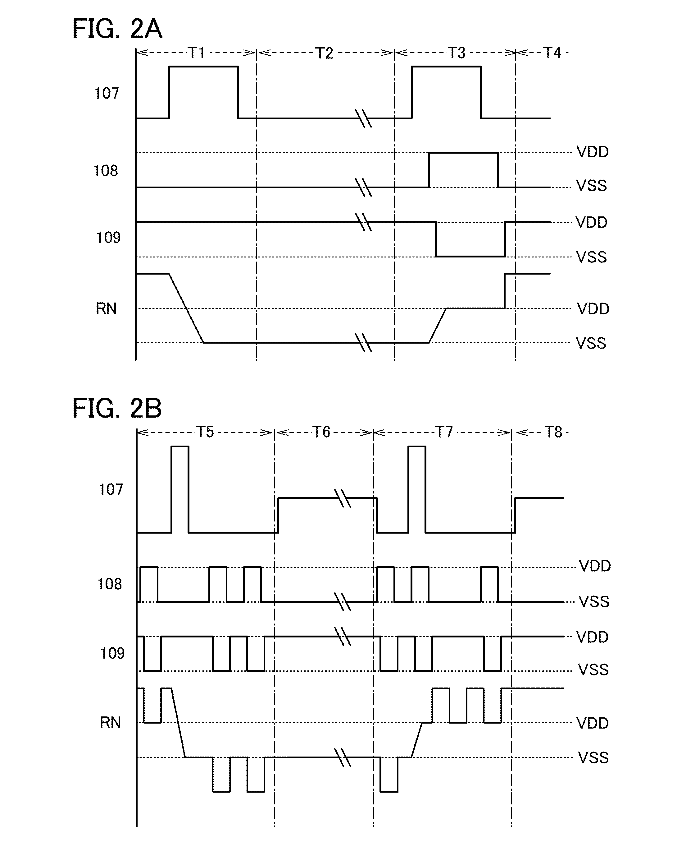
[0048]FIG. 1A illustrates a semiconductor device 101 of one embodiment of the present invention. The semiconductor device 101 of one embodiment of the present invention includes a plurality of (preferably greater than or equal to 10, more preferably greater than or equal to 100) logic circuits 102 arranged in a matrix. The logic circuits 102 are each electrically connected to a high potential power source and a low potential power source. The logic circuits 102 are electrically connected to the low potential power source through a low potential power supply line 110. A programming element 103 is provided between the low potential power supply line 110 and the logic circuit 102 so as to be connected in series with the logic circuit 102. The programming element 103 controls connection states betw...
embodiment 2
[0186]In this embodiment, an example of a cross-sectional structure of the semiconductor device described in Embodiment 1 is described with reference to FIG. 9.
[0187]FIG. 9 illustrates an example in which the first transistor 104 overlaps the second transistor 105 and the capacitor 106 overlaps the first transistor 104. With such a planar layout, the area occupied by the semiconductor device can be reduced, which leads to higher integration.
[0188]In FIG. 9, the second transistor 105 is provided over a substrate 1000. The single crystal silicon substrate imparting n-type conductivity is used as the substrate 1000, and an impurity element imparting n-type conductivity is added to form an n-type impurity region 1044 functioning as a lightly doped drain (LDD) region or an extension region and an n-type impurity region 1045 functioning as a source region or a drain region. The second transistor 105 is an n-channel transistor and includes a channel formation region 1043, the n-type impuri...
embodiment 3
[0260]In this embodiment, a configuration of a CPU, which is a semiconductor device according to one embodiment of the present invention is described.
[0261]FIG. 10 illustrates a configuration of the CPU of this embodiment. The CPU in FIG. 10 mainly includes an ALU 9901, an ALU controller 9902, an instruction decoder 9903, an interrupt controller 9904, a timing controller 9905, a register 9906, a register controller 9907, a bus I / F 9908, a rewritable ROM 9909, and a ROM I / F 9920, over a substrate 9900. Note that “ALU” means “arithmetic logic unit”, the “bus I / F” means “bus interface”, and the “ROM I / F” means “ROM interface”. The ROM 9909 and the ROM I / F 9920 may be provided over another chip. Obviously, the CPU illustrated in FIG. 10 is just an example in which the structure is simplified, and an actual CPU may have various structures depending on the application.
[0262]An instruction which is input to the CPU through the Bus I / F 9908 is input to the instruction decoder 9903 and decod...
PUM
 Abstract
Description
Claims
Application Information