Uicc encapsulated in printed circuit board of wireless terminal

a wireless terminal and printed circuit board technology, applied in the field of radio communication, can solve the problems of wireless terminal theft, undesirable loss or theft of uicc or similar identity modules,

Inactive Publication Date: 2013-11-07
SIERRA WIRELESS
View PDF9 Cites 36 Cited by
  • Summary
  • Abstract
  • Description
  • Claims
  • Application Information

AI Technical Summary

Benefits of technology

[0009]An object of the present technology is to provide a UICC encapsulated in printed circuit board of a wireless terminal. In accordance with an aspect of the present technology, there is provided a multilayer circuit board of a wireless terminal, the wireless terminal utilizing a UICC, the multilayer circuit board comprising one or more interior layers and configured to accommodate: a UICC encapsulated within at least one of the one or more interior layers of the multilayer circuit board; and one or more additional components integral to functionality of the wireless terminal.
[0010]In accordance with another aspect of the present technology, there is provided a circuit assembly of a wireless terminal utilizing a UICC, the circuit assembly comprising a multilayer circuit board, the multilayer circuit board comprising one or more interior layers and configured to accommodate: a UICC encapsulated within at least one of the one or more interior layers of the multilayer circuit board; and one or more additional components integral to functionality of the wireless terminal, the circuit assembly further comprising the UICC and the additional components operatively coupled to the multilayer circuit board.
[0011]In accordance with another aspect of the present technology, there is provided a wireless terminal comprising a multilayer circuit board, the multilayer circuit board comprising one or more interior layers and configured to accommodate: a UICC encapsulated within at least one of the one or more interior layers of the multilayer circuit board; and one or more additional components integral to functionality of the wireless terminal.
[0012]In accordance with another aspect of the pre

Problems solved by technology

As such, it is undesirable that a UICC or similar identity module should be lost or stolen.
Similarly, wireless terminals are valuable technology, and it is undesirab

Method used


Image

  • Uicc encapsulated in printed circuit board of wireless terminal
  • Uicc encapsulated in printed circuit board of wireless terminal
  • Uicc encapsulated in printed circuit board of wireless terminal

Examples


example 1

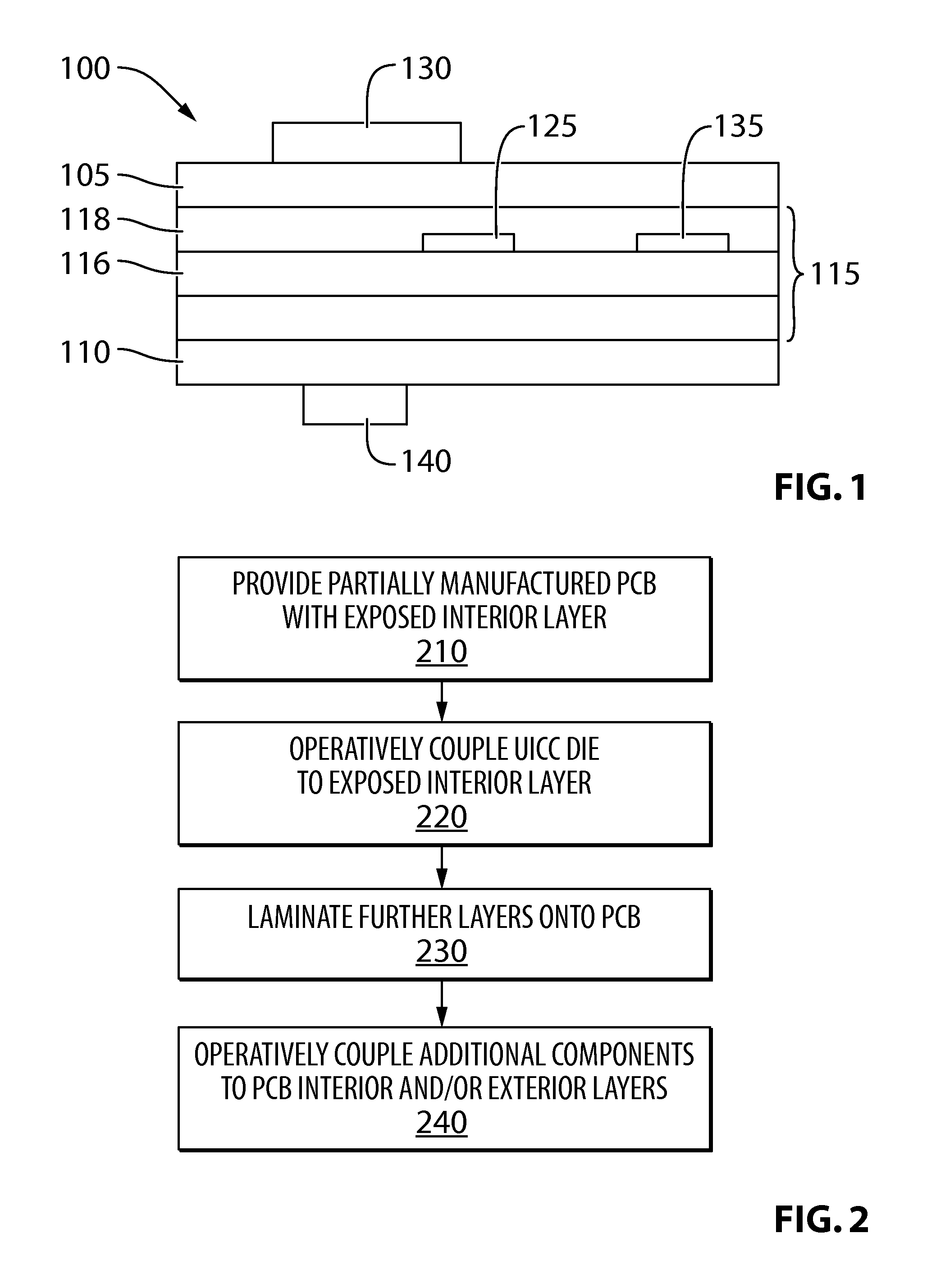
[0057]FIG. 1 illustrates a cross-sectional side view of a PCB 100 comprising two exterior layers 105 and 110, and at least one interior layer 115. Dimensions of FIG. 1 are exaggerated for clarity. The PCB 100 is made to be a component of a wireless terminal (not shown), which accommodates the UICC as well as at least one other electronic component providing a function of the wireless terminal, such as digital signal processing, digital logic, data storage, analog amplification, power management, modulation, radio transmission, radio reception, machine or user interface, and the like, as would be readily understood by a worker skilled in the art. In one embodiment, the PCB may accommodate components associated with substantially all or at least a significant portion of functions of the wireless terminal.

[0058]The interior layer 115 comprises a UICC die 125, for example provided within an aperture within the interior layer. The interior layer 115 comprises a layer 116 onto which condu...

example 2

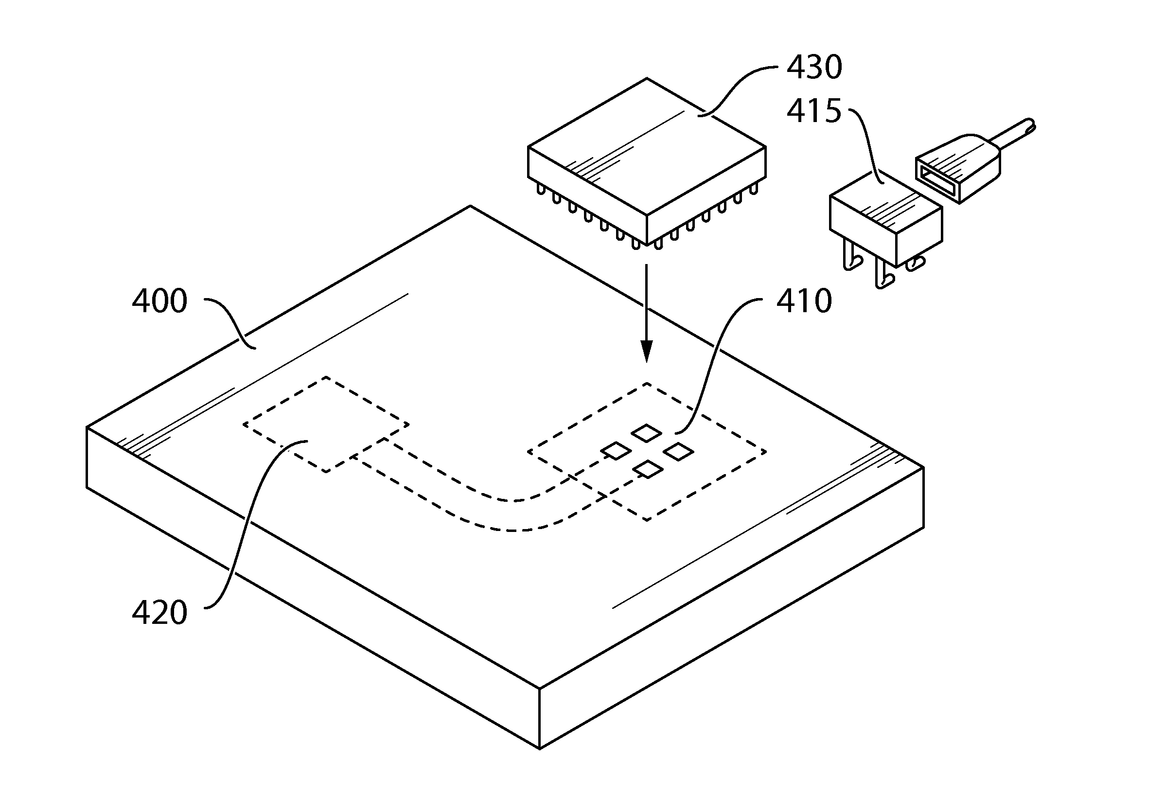
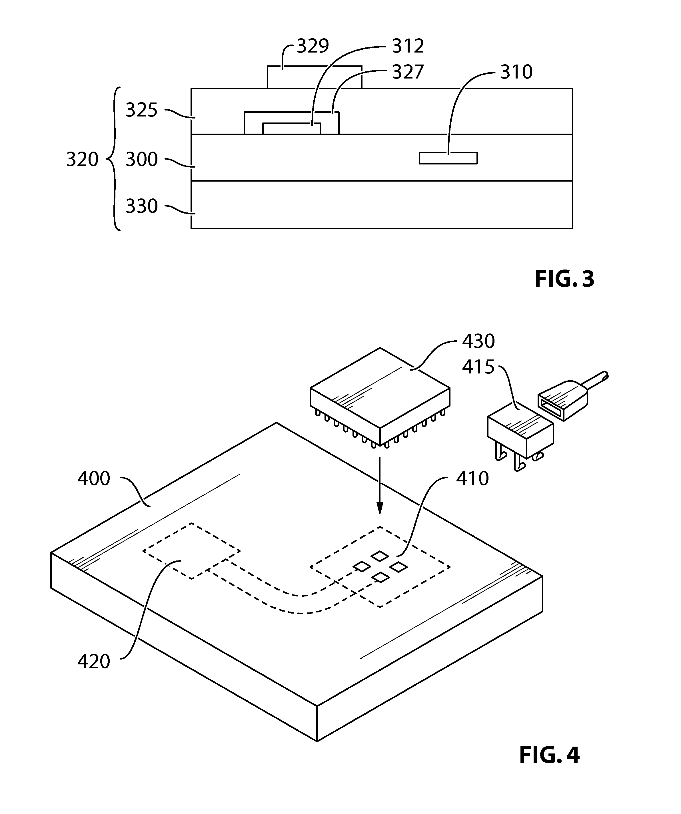
[0060]FIG. 2 illustrates a method of manufacturing a circuit assembly comprising a multilayer PCB and an encapsulated UICC, in accordance with embodiments of the present technology. As illustrated, the method comprises providing 210 a partially manufactured PCB with an exposed interior layer; operatively coupling 220 a UICC die to the exposed interior layer; laminating 230 further layers onto the PCB; and operatively coupling 240 additional components to PCB interior and / or exterior layers. Various operations involved with each step may be performed in a manner as would be readily understood by a worker skilled in the art. Operative coupling of additional components such as semiconductor dies to interior layers of the PCB may be performed during manufacture of the PCB, when the appropriate interior layer is exposed and before further layers are added.

example 3

[0061]FIG. 3 illustrates a cross-sectional side view of a multilayer circuit board 300 comprising an encapsulated UICC 310, along with adjacent circuit boards 325, 330, in accordance with an embodiment of the present technology. The multilayer circuit board 300 is an interposer board forming part of a stacked board assembly 320. The stacked board assembly 320 comprises one or more additional PCBs, such as PCBs 325 and 330. The PCBs 300, 325 and 330 are mechanically and electrically interconnected, for example using adhesive, mating connectors, solder, or the like, or a combination thereof. Each of the PCBs 300, 325 and 330 may comprise mating connectors, solder pads, or the like, on the surfaces thereof for interconnection. Additionally, the PCBs 325 and 330 need not be multilayer circuit boards having an interior layer, but may comprise and / or be populated only on a top layer, only on a bottom layer or only on top and bottom layers.

[0062]It is also contemplated that the UICC 310 ma...


PUM


Abstract

A multilayer circuit board of a wireless terminal, a circuit assembly comprising the circuit board and a wireless terminal comprising the circuit assembly are provided. The wireless terminal is of a type which utilizes a UICC. The multilayer circuit board is configured to accommodate a UICC encapsulated within one or more interior layers of the multilayer circuit board, for example as a semiconductor die. The multilayer circuit board is further configured to accommodate one or more additional components integral to functionality of the wireless terminal, optionally also embedded within the circuit board. Integration of components into the interior layers may facilitate theft deterrence and/or tamper resistance. A physical programming interface to the encapsulated UICC may be rendered inaccessible after initial programming.

Description

BACKGROUND OF THE INVENTION[0001]1. Field of the Invention[0002]The present technology pertains in general to radio communication using terminals comprising Universal Integrated Circuit Card (UICC), Subscriber Identity Module (SIM) or the like.[0003]2. Description of the Related Art[0004]Conventionally, a UICC is an external and removable element in relation to the communication terminal with which it is associated. This is because its aim is to identify a “subscriber” who may decide to change terminals without wishing to change his identifier associated with the UICC. The latter is therefore arranged in a housing provided in the communication device.[0005]UICCs contain valuable information usable for accessing wireless networks. As such, it is undesirable that a UICC or similar identity module should be lost or stolen. UICC theft can be regarded as a type of identity theft. Similarly, wireless terminals are valuable technology, and it is undesirable that a wireless terminal should ...

Claims


Application Information

Patent Timeline
IPC IPC(8): H05K1/18
CPCH05K1/185H05K1/0275H05K1/0293H05K3/4697H05K2201/10098H05K2201/10181
Inventor SYAL, ASHISH
Owner SIERRA WIRELESS
Why Eureka
Try Eureka