Method for Bit-Error Rate Testing of Resistance-based RAM Cells Using a Reflected Signal

Active Publication Date: 2013-11-07
AVALANCHE TECH
View PDF4 Cites 17 Cited by
  • Summary
  • Abstract
  • Description
  • Claims
  • Application Information

AI Technical Summary

Problems solved by technology

Detection of such very low BER values requires a comparably large number of switching attempts and reading operations which can require elapsed times that are impractical and/or too cos

Method used


Image

  • Method for Bit-Error Rate Testing of Resistance-based RAM Cells Using a Reflected Signal
  • Method for Bit-Error Rate Testing of Resistance-based RAM Cells Using a Reflected Signal
  • Method for Bit-Error Rate Testing of Resistance-based RAM Cells Using a Reflected Signal

Examples


Embodiment Construction

[0025]In the following description of the embodiments, reference is made to the accompanying drawings that form a part hereof, and in which is shown by way of illustration of the specific embodiments in which the invention may be practiced. It should be noted that the figures discussed herein are not drawn to scale.

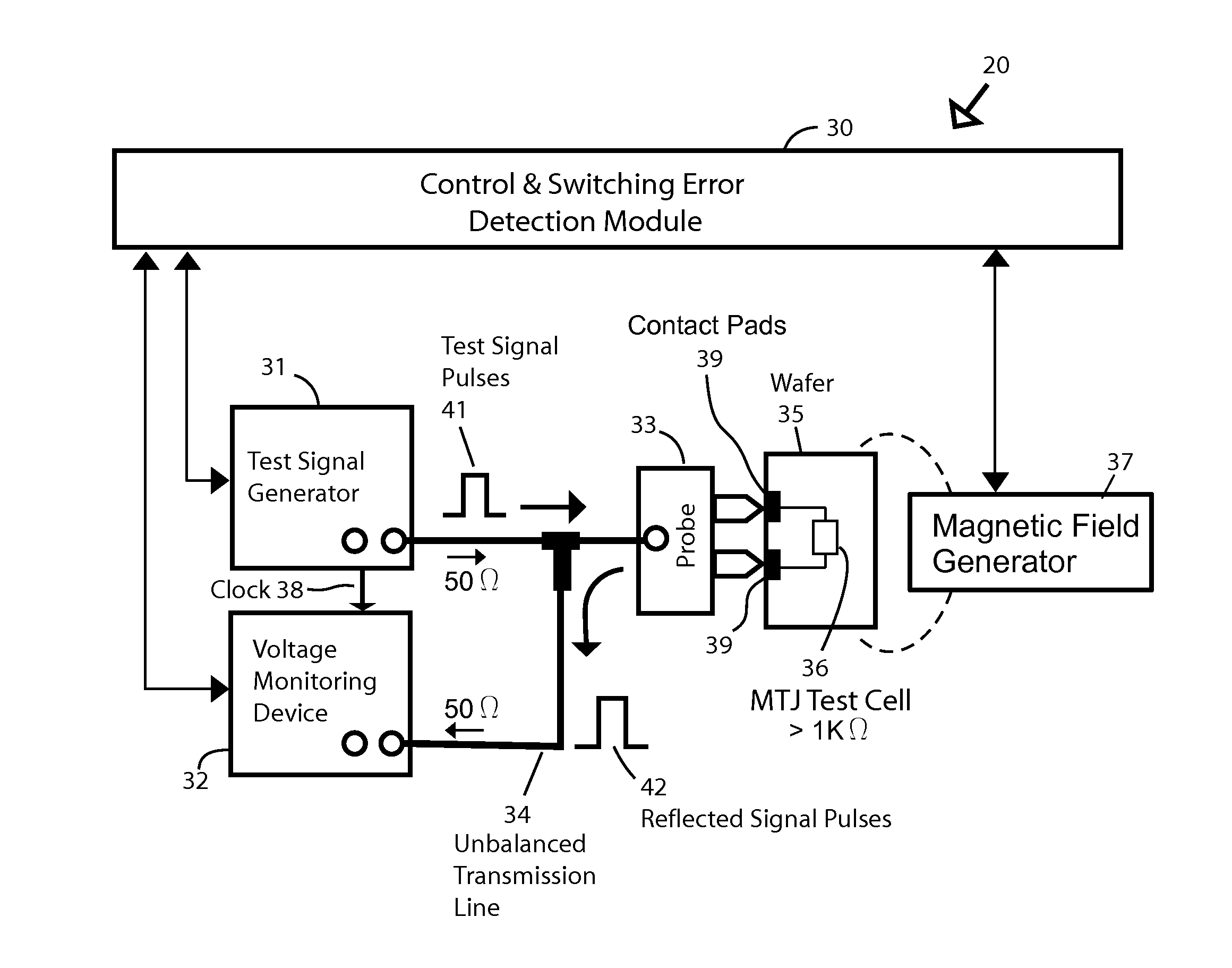
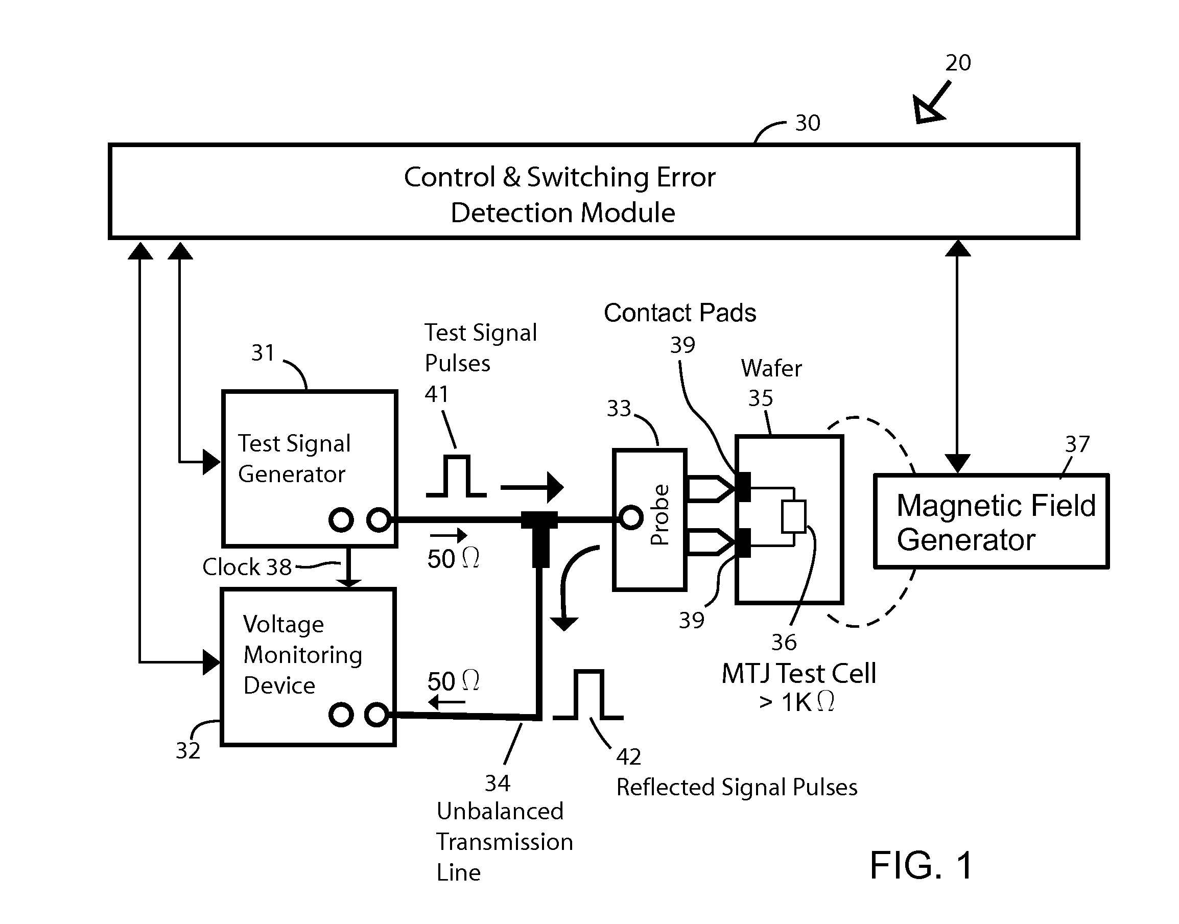
[0026]A test system 20 for an embodiment of the invention for testing an MTJ memory cell is illustrated in FIG. 1. In this example test wafer 35 has been fabricated with MTJ test cell 36. The top and bottom electrodes (not shown) are directly connected to the two contact pads 39 on the surface of the wafer. The wafer can also have other MTJ test cells on it, and it can also have production MTJ-MRAM arrays with complete CMOS logic. As shown, two points on the electrical signal probe 33 are positioned in electrical contact with the two contact pads 39. The electrical signal probe 33 can be a standard commercially available multipoint probe. The mechanical test platform, whi...


PUM


Abstract

A testing method is described for performing a fast bit-error rate (BER) measurement on resistance-based RAM cells, such MTJ cells, at the wafer or chip level. Embodiments use one or more specially designed test memory cells fabricated with direct electrical connections between the two electrodes of the cell and external contact pads (or points) on the surface of the wafer (or chip). In the test setup the memory cell is connected an impedance mismatched transmission line through a probe for un-buffered, fast switching of the cell between the high and low resistance states without the need for CMOS logic to select and drive the cell. The unbalanced transmission line is used generate signal reflections from the cell that are a function of the resistance state. The reflected signal is used to detect whether the test cell has switched as expected.

Description

FIELD OF THE INVENTION[0001]The present invention relates to the techniques for testing or screening memory cells that use distinct resistance states to store data such as magnetic random access memory (MRAM), phase change RAM, resistive RAM, and Memristors.BACKGROUND OF THE INVENTION[0002]The data storage component of an STT-MRAM (Spin Torque Transfer Magnetic Random Access memory) is a magnetic tunnel junction (MTJ) cell. The write operation uses electrical current to switch the magnetization direction of the free layer (storage layer) relative to that of the reference layer of the MTJ.[0003]A typical type of magnetoresistive random access memory (MRAM) cell including a magnetic tunnel junctions (MTJ) will be described as examples of devices that can be used with the method of the invention. An MTJ can be designed for in-plane or perpendicular magnetization of the MTJ layer structure with respect to the film surface. The MTJ includes a free magnetic layer, a nonmagnetic spacer or ...

Claims


Application Information

Patent Timeline
IPC IPC(8): G11C11/00
CPCG11C11/16G11C13/00G11C29/08G11C29/50G11C29/56008G11C29/56016G11C2029/5602G11C29/44G11C29/50008
Inventor WANG, ZIHUIZHOU, YUCHENZHANG, JINGHUAI, YIMING
Owner AVALANCHE TECH
Why Eureka
Try Eureka