Circuit technique to electrically characterize block mask shifts

a technology of mask shift and circuit, applied in the field of electrical and electronic arts, can solve problems such as deviation of actual on-wafer pattern from the designed circuit layou

Inactive Publication Date: 2013-12-05
GLOBALFOUNDRIES INC
View PDF1 Cites 8 Cited by
  • Summary
  • Abstract
  • Description
  • Claims
  • Application Information

AI Technical Summary

Benefits of technology

The patent text describes a method for characterizing the performance of an integrated circuit design by measuring the difference in threshold voltage between transistors. This is done by creating a physical test circuit with multiple repeating circuit structures, where the transistors are deliberately offset from their normal location. The method also includes measuring the threshold voltage difference between actual transistors on an actual integrated circuit and correlating it to the results of testing on the proposed integrated circuit design. The invention also provides on-chip monitoring circuitry and computer programs for carrying out the method steps. The technical effect of the invention is to provide a reliable and efficient way to characterize the performance of integrated circuit designs.

Problems solved by technology

With technology scaling, process imperfections result in deviation of actual on-wafer patterns from the designed circuit layout.
This is due to the extremely dense layouts and very stringent ground rules associated with SRAMs.

Method used


Image

  • Circuit technique to electrically characterize block mask shifts
  • Circuit technique to electrically characterize block mask shifts
  • Circuit technique to electrically characterize block mask shifts

Examples


Embodiment Construction

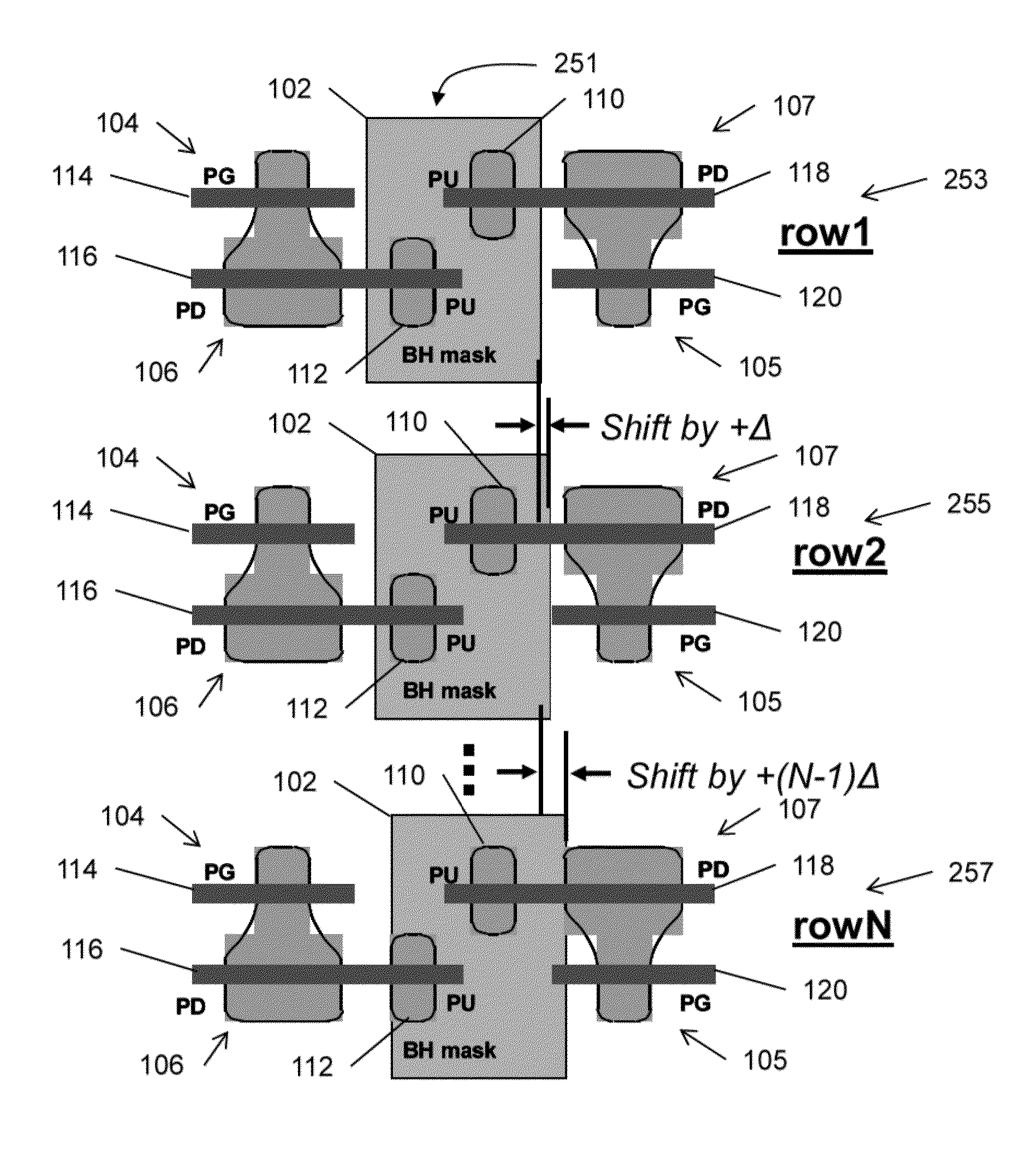
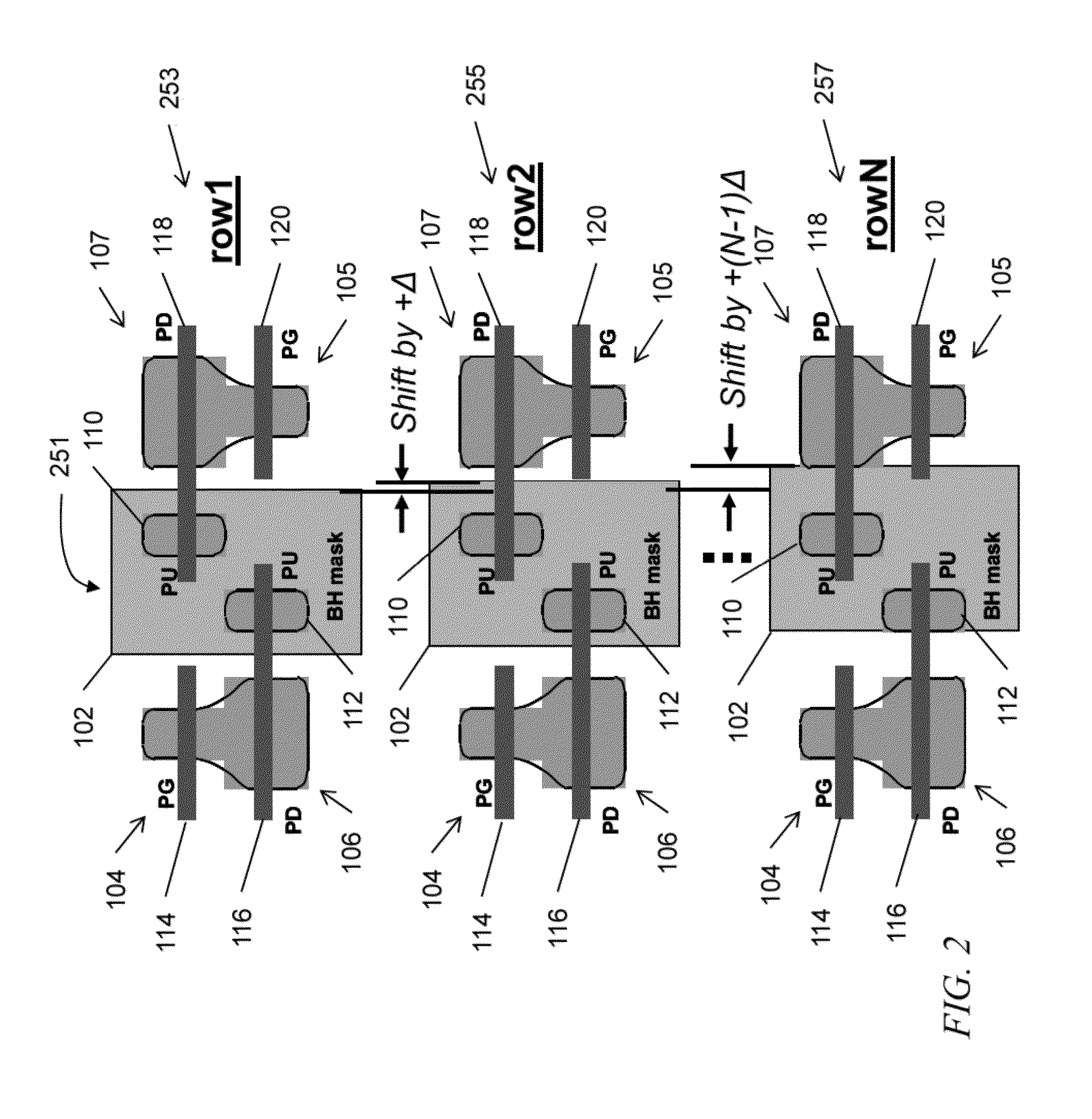
[0032]As noted, in the field of integrated circuit (IC) fabrication, technology scaling continues; i.e., the size of circuit features continues to decrease. With technology scaling, process imperfections result in deviation of actual on-wafer patterns from the designed circuit layout. To fabricate a layout, each wafer has to go through patterning of several layers to fabricate transistors, contacts and interconnects. A tool has to physically pick a mask and align it with the wafer to fabricate the desired pattern. With minimum feature size on a wafer scaled to less than 30 nm, the alignment tolerance is typically reduced to less than 5 nm for several significant layers. Static Random Access Memories (SRAMs) are an example of a type of circuit that is particularly vulnerable to this kind of impact. This is due to the extremely dense layouts and very stringent ground rules associated with SRAMs.

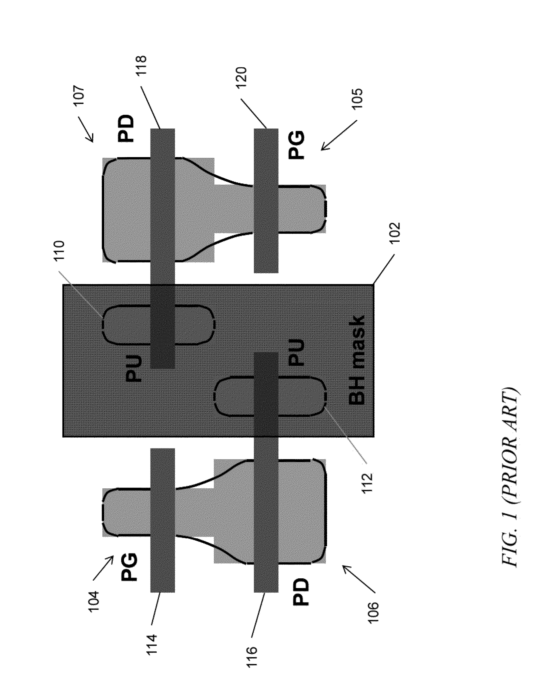
[0033]For example, FIG. 1 shows an exemplary layout of a 6-transistor SRAM cell, as known i...


PUM


Abstract

A physical test integrated circuit has a plurality of repeating circuit portions corresponding to an integrated circuit design. A first of the portions is fabricated with a nominal block mask location, and additional ones of the portions are deliberately fabricated with predetermined progressive increased offset of the block mask location from the nominal block mask location. For each of the portions, the difference in threshold voltage between a first field effect transistor and a second field effect transistor is determined. The predetermined progressive increased offset of the block mask location is in a direction from the first field effect transistor to the second field effect transistor. The block mask overlay tolerance is determined at a value of the progressive increased offset corresponding to an inflection of the difference in threshold voltage from a zero difference. A method for on-chip monitoring, and corresponding circuits, are also disclosed.

Description

STATEMENT OF GOVERNMENT RIGHTS[0001]Not Applicable.CROSS-REFERENCE TO RELATED APPLICATIONS[0002]Not Applicable.FIELD OF THE INVENTION[0003]The present invention relates to the electrical and electronic arts, and, more particularly, to circuit testing and fabrication techniques and the like.BACKGROUND OF THE INVENTION[0004]In the field of integrated circuit (IC) fabrication, technology scaling continues; i.e., the size of circuit features continues to decrease. With technology scaling, process imperfections result in deviation of actual on-wafer patterns from the designed circuit layout. To fabricate a layout, each wafer has to go through patterning of several layers to fabricate transistors, contacts and interconnects. A tool has to physically pick a mask and align it with the wafer to fabricate the desired pattern. With minimum feature size on a wafer scaled to less than 30 nm, the alignment tolerance is typically reduced to less than 5 nm for several significant layers. Static Ran...

Claims


Application Information

Patent Timeline
Patent Type & Authority Applications(United States)
IPC IPC(8): H01L21/66H01L23/50
CPCH01L2924/0002H01L22/34H01L2924/00H10B10/12H01L22/14H01L27/0203
Inventor ACAR, EMRAHBANSAL, ADITYACHIDAMBARRAO, DURESETIPANG, LIANG-TECKSINGHEE, AMITH
Owner GLOBALFOUNDRIES INC
Why Eureka
Try Eureka