Solid-state imagingelement, calibration method of solid-state imagingelement, shutter device, and electronic apparatus

a technology of solid-state imaging and calibration method, which is applied in the direction of radio frequency control devices, instruments, television systems, etc., can solve the problems of large wavelength errors, difficult control of wavelength variations, and inability to freely modulate the wavelength of light that can pass through the dielectric laminated film

Inactive Publication Date: 2013-12-19
SONY SEMICON SOLUTIONS CORP
View PDF7 Cites 34 Cited by
  • Summary
  • Abstract
  • Description
  • Claims
  • Application Information

AI Technical Summary

Benefits of technology

[0015]According to the present disclosure, it is possible to obtain a solid-state imaging element that can perform imaging in the ranges from the near-infrared region to the visible light region and which allows an amount of received light to be adjusted, a calibration method of the solid

Problems solved by technology

Hence, the wavelengths of light that can pass through the dielectric laminated film cannot be modulated freely.
Further, it is difficult to control variations in wavelength due to variations in film thickness of the dielectric laminated film, and there are large wavelength errors in reg

Method used


Image

  • Solid-state imagingelement, calibration method of solid-state imagingelement, shutter device, and electronic apparatus
  • Solid-state imagingelement, calibration method of solid-state imagingelement, shutter device, and electronic apparatus
  • Solid-state imagingelement, calibration method of solid-state imagingelement, shutter device, and electronic apparatus

Examples


first embodiment

Example of Solid-State Imaging Element

[0054]FIG. 3 is a schematic block diagram showing the whole of a solid-state imaging element 11 according to a first embodiment of the present disclosure. The solid-state imaging element 11 according to the example of the present embodiment includes a pixel section 13 formed by a plurality of pixels 12 arranged on a substrate 21 made of silicon, a vertical driving circuit 14, column signal processing circuits 15, a horizontal driving circuit 16, an output circuit 17, a control circuit 18, and the like. The pixels 12 include a photoelectric conversion section formed by a photodiode, a charge accumulating capacitance section, and a plurality of MOS transistors, and the plurality of pixels 12 are arranged regularly in the form of a two-dimensional array on the substrate 21. The MOS transistors forming the pixels 12 may be four MOS transistors, that is, a transfer transistor, a reset transistor, a selecting transistor, and an amplifying transistor, ...

first modification

[First Modification]

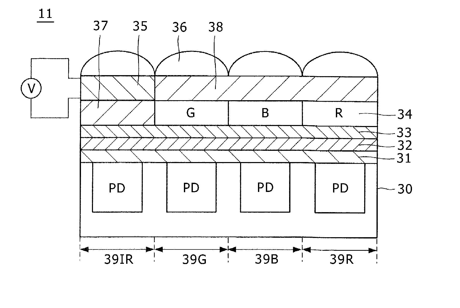
[0084]FIG. 9 is a schematic sectional view of four pixels of a solid-state imaging element 41 according to the first modification.

[0085]In FIG. 9, parts corresponding to those of FIG. 4 are identified by the same reference symbols, and repeated description thereof will be omitted. As shown in FIG. 9, the solid-state imaging element 41 according to the modification has an IR cutoff filter 42 over a red pixel 39R, a green pixel 39G, and a blue pixel 39B other than an IR pixel 39IR.

[0086]The solid-state imaging element 41 cuts off light of wavelengths in the infrared region in the red pixel 39R, the green pixel 39G, and the blue pixel 39B provided with the IR cutoff filter 42. Therefore, signal components obtained in the visible light pixels are signal components resulting from light in the visible light region, but include a noise component ΔE resulting from a dark current.

[0087]Accordingly, the solid-state imaging element 41 also corrects dark current nonuniformit...

second modification

[Second Modification]

[0092]The nano-carbon laminated film can change a wavelength region of light that the nano-carbon laminated film can transmit (in which region transmittance can be modulated) and light transmittance thereof according to the constitution and material of the nano-carbon laminated film. FIG. 10 is a schematic sectional view of a nano-carbon laminated film according to a second modification. As shown in FIG. 10, the nano-carbon laminated film 45 includes a first electrode 46, a dielectric layer 47, and a second electrode 48.

[0093]The first electrode 46 and the second electrode 48 are each formed by one nano-carbon layer or a plurality of nano-carbon layers. In addition, in the second modification, graphene, for example, is used as the nano-carbon layers forming the first electrode 46 and the second electrode 48. A voltage power supply V is connected to the first electrode 46 and the second electrode 48 via wiring.

[0094]The dielectric layer 47 is provided between the...


PUM


Abstract

Disclosed herein is a solid-state imaging element including: a plurality of pixels including a photoelectric conversion section; and a nano-carbon laminated film disposed on a side of a light receiving surface of the photoelectric conversion section and formed with a plurality of nano-carbon layers, transmittance of light and a wavelength region of transmissible light changing in the nano-carbon laminated film according to a voltage applied to the nano-carbon laminated film.

Description

BACKGROUND[0001]The present technology relates to a solid-state imaging element including a nano-carbon laminated film, a calibration method of the solid-state imaging element, and an electronic apparatus using the solid-state imaging element. Further, the present technology relates to a shutter device including a nano-carbon laminated film and an electronic apparatus including the shutter device.[0002]A solid-state imaging element typified by a CCD (Charge Coupled Device) image sensor and a CMOS (Complementary Metal Oxide Semiconductor) image sensor includes a photoelectric conversion section formed by a photodiode formed on the side of a light receiving surface of a substrate and a charge transfer section. In such a solid-state imaging element, the photodiode subjects light incident on the sensor section to photoelectric conversion to generate a signal charge. Then, the charge transfer section transfers the generated signal charge, and outputs the signal charge as a video signal. ...

Claims


Application Information

Patent Timeline
IPC IPC(8): H01L27/146G02F1/01
CPCH01L27/146G02F1/01B82Y20/00G02F1/015H01L27/1462H04N2209/047H01L27/14645B82Y30/00H04N5/238H04N5/35545H04N5/361H01L27/14625H04N23/75H04N25/581H04N25/63
Inventor IZUHA, KYOKOKADONO, KOJIHARADA, KOUICHIKOBAYASHI, TOSHIYUKI
Owner SONY SEMICON SOLUTIONS CORP
Why Eureka
Try Eureka