Thickness monitoring device, etching depth monitoring device and thickness monitoring method

Inactive Publication Date: 2013-12-19
SHIMADZU CORP
View PDF2 Cites 4 Cited by
  • Summary
  • Abstract
  • Description
  • Claims
  • Application Information

AI Technical Summary

Benefits of technology

The invention provides a device and method for monitoring the thickness of an object in real-time using a relatively narrow band light source. This technology is able to extract the change in thickness of an object by analyzing the interference light from multiple single-wavelength components. This allows for accurate thickness measurement, even when using a narrow band light source. The method is also able to reduce the effect of distortion or noise in the observed spectrum, resulting in high precision thickness measurement.

Problems solved by technology

However, in the aforementioned Patent Literature 1, it is necessary to employ a wide band spectrometer compatible with the wide band tungsten lamp, so there is the problem that the influence of chromatic aberration of the optical system is substantial and the design of the optical system becomes difficult.
Furthermore, with a wide band light source such as a tungsten lamp, compared to a single wavelength light source such as a laser, the luminance is low, and the sensor exposure time has to be made longer at the time of measurement.
Thus, there is the problem that thickness measurement takes a long time, making it difficult to perform real-time thickness monitoring.
However, it is generally known that the uncertainty of analysis based on spectral interference fringes is determined by the inverse of the frequency band of the light source, and hardly any difference that would allow the discrimination of thickness on the order of several μm, as in an etching mask or the like, appears in an interference spectrum obtained from a relatively narrow band light source.
However, observed spectra which are actually obtained contain distortion and noise due to the effects of the emission spectrum of the light source itself, the bias spectrum due to the optical system, and other interference light components.
Thus, even if curve fitting is performed on the observed interference spectrum, variability in the measured thickness values occurs due to spectrum distortion, and measuring the true thickness of the object of measurement with high precision is difficult.

Method used


Image

  • Thickness monitoring device, etching depth monitoring device and thickness monitoring method
  • Thickness monitoring device, etching depth monitoring device and thickness monitoring method
  • Thickness monitoring device, etching depth monitoring device and thickness monitoring method

Examples


Embodiment Construction

[0036]A specific mode of embodiment of the present invention will be described below based on the drawings.

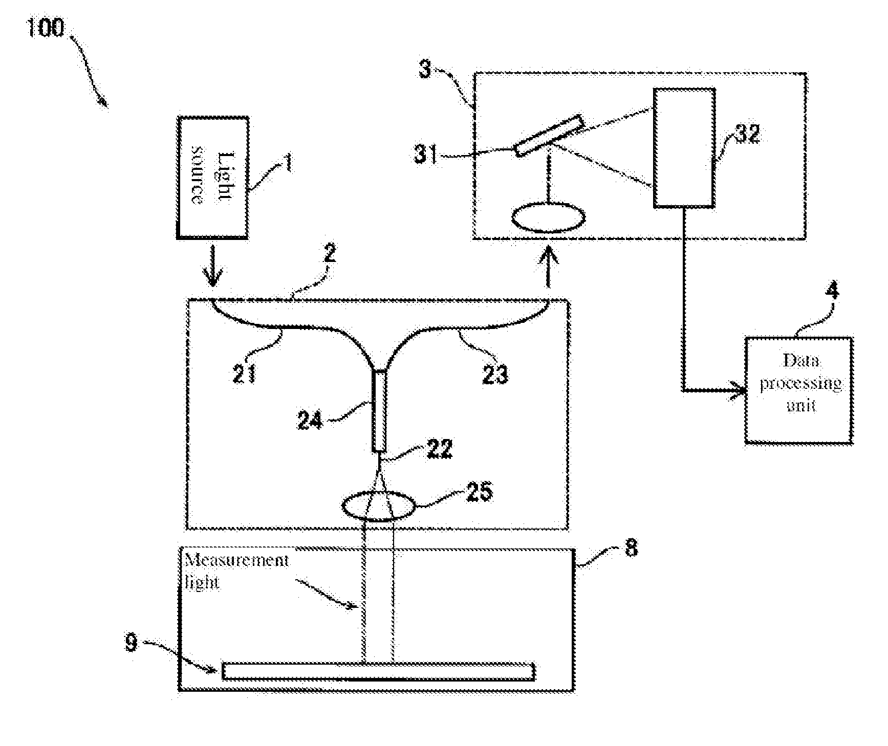
[0037]First, referring to FIG. 1 and FIG. 2, the overall configuration of an etching monitoring device 100 according to a mode of embodiment of the present invention will be described. In the present mode of embodiment, an example will be described in which the present invention has been applied to an etching monitoring device 100 which constitutes an example of a thickness monitoring device and etching depth monitoring device.

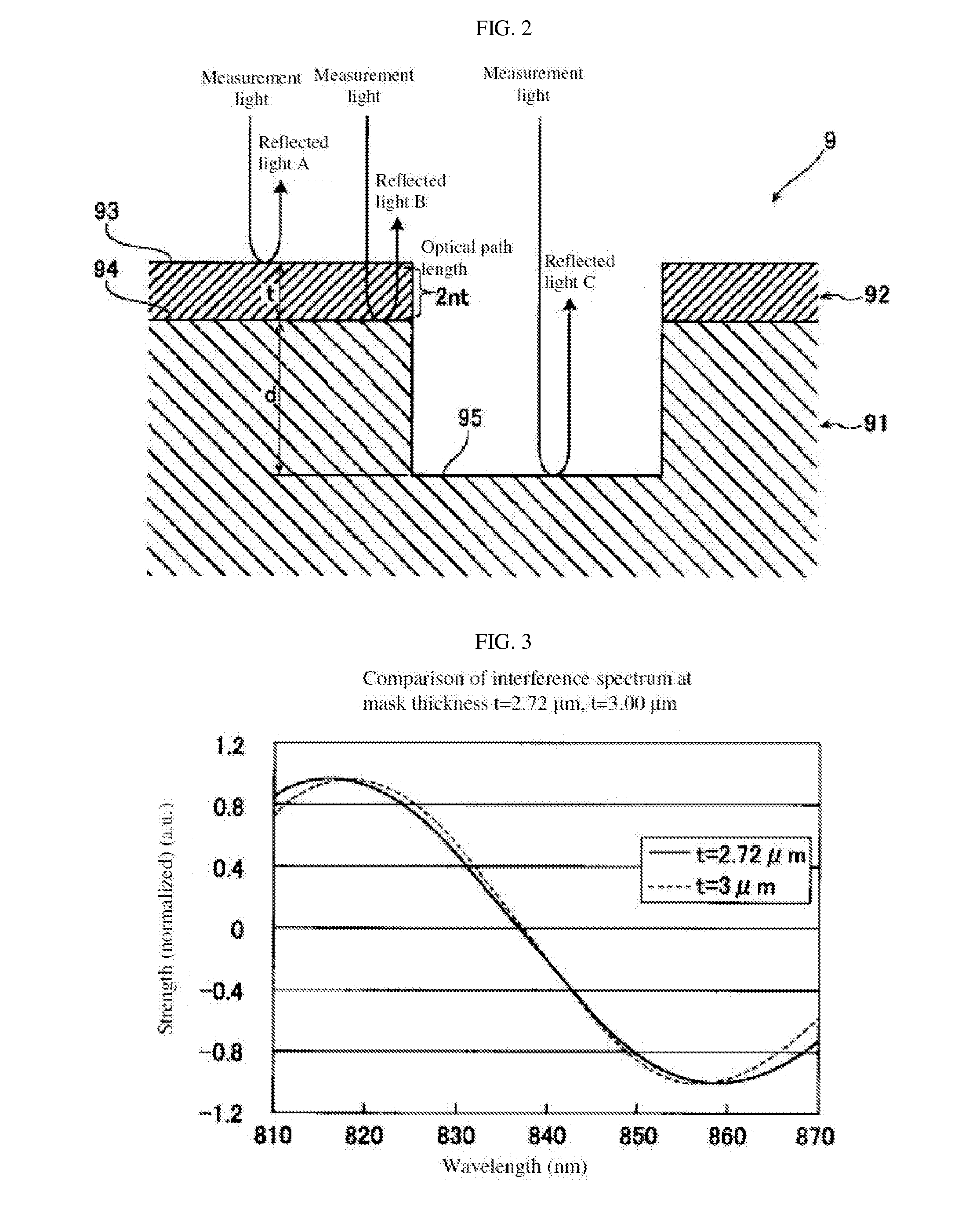
[0038]The etching monitoring device 100 according to the present mode of embodiment is a device which measures, in real time, a distance (depth, thickness) which changes moment to moment, for example, the depth of a trench being formed in a specimen 9 undergoing etching by a plasma etching device. As shown in FIG. 2, specimen 9 comprises a substrate 91 composed of silicon, and an etching mask (hereinafter referred to as “mask”) 92 formed in a predetermine...


PUM


Abstract

A thickness monitoring device capable of performing thickness measurement of an object of measurement in real time even when using a relatively narrow band light source. This etching monitoring device (thickness monitoring device) includes a light source which produces measurement light having a predetermined wavelength bandwidth; an array detector which detects, for each wavelength, interference light of measurement light reflected from mask, whereof the thickness changes over time; and data processing unit which computes the thickness of the mask based on change over time of a plurality of single-wavelength components of the interference light detected by the array detector.

Description

TECHNICAL FIELD[0001]The present invention relates to a thickness monitoring device, etching depth monitoring device and thickness monitoring method, particularly to a thickness monitoring device, etching depth monitoring device and thickness monitoring method using interference light.BACKGROUND ART[0002]A mask thickness monitoring device which measures the thickness of an etching mask (object of measurement) using interference light is known in the prior art (for example, see Patent Literature 1).[0003]The aforementioned Patent Literature 1 discloses a mask thickness monitoring device comprising a tungsten lamp which irradiates a specimen, wherein an etching mask has been formed on a silicon wafer, with measurement light; a spectrometer which detects interference light due to light reflected from the etching mask and outputs a spectrometric spectrum; and a mask thickness computation unit which computes the mask thickness based on curve fitting of a theoretical waveform and a spectr...

Claims


Application Information

Patent Timeline
IPC IPC(8): G01B11/06
CPCG01B11/0675G01B11/0633
Inventor GOTO, HIROOMINAGUMO, YUZOKATO, RUI
Owner SHIMADZU CORP
Why Eureka
Try Eureka