

Sputtering target and method for using the same
a technology of sputtering target and target, which is applied in the direction of electrolysis components, vacuum evaporation coatings, coatings, etc., can solve the problems of unstable physical properties and easy amorphous oxidized semiconductor films, and achieve high crystallinity, high reliability of semiconductor devices, and stable electric characteristics
- Summary
- Abstract
- Description
- Claims
- Application Information
AI Technical Summary
Benefits of technology
Problems solved by technology
Method used
Image

Examples
embodiment 1
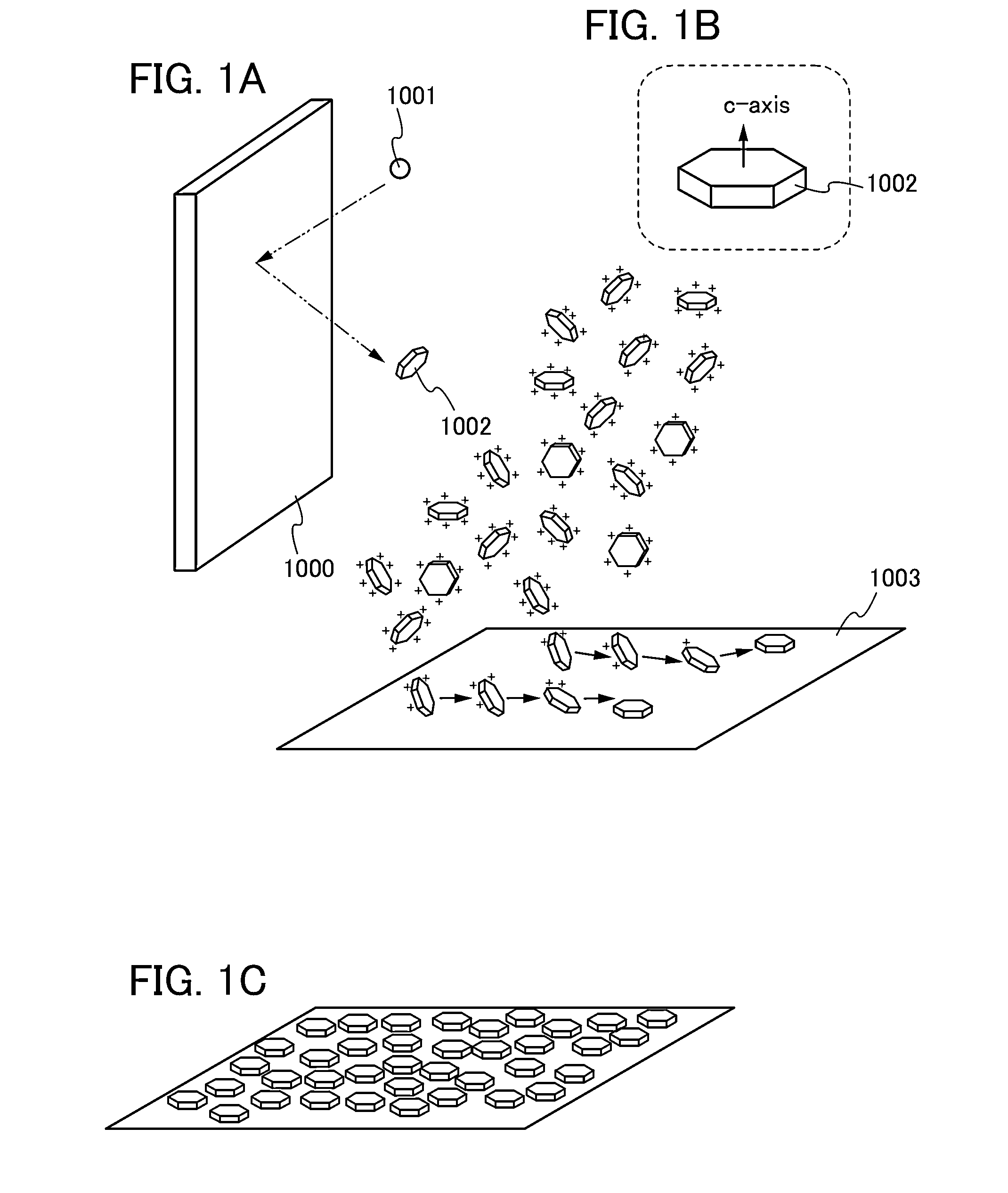
[0148]In this embodiment, a sputtering target of one embodiment of the present invention will be described.
[0149]The sputtering target includes a polycrystalline oxide containing a plurality of crystal grains whose average grain size is less than or equal to 3 μm, preferably less than or equal to 2.5 μm, further preferably less than or equal to 2 μm.
[0150]Alternatively, the sputtering target includes a polycrystalline oxide containing a plurality of crystal grains, in which the proportion of crystal grains whose grain size is greater than or equal to 0.4 μm and less than or equal to 1 μm is 8% or higher, preferably 15% or higher, further preferably 25% or higher.
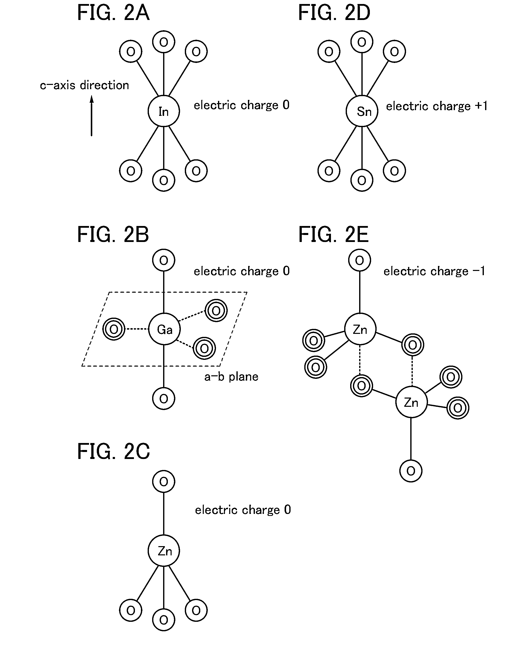
[0151]Further, the plurality of crystal grains included in the sputtering target have cleavage planes. The cleavage plane is a plane parallel to an a-b plane, for example.
[0152]The relative density of the sputtering target is higher than or equal to 90%, higher than or equal to 95%, or higher than or equal to 99%.
[0153]Owing...
embodiment 2
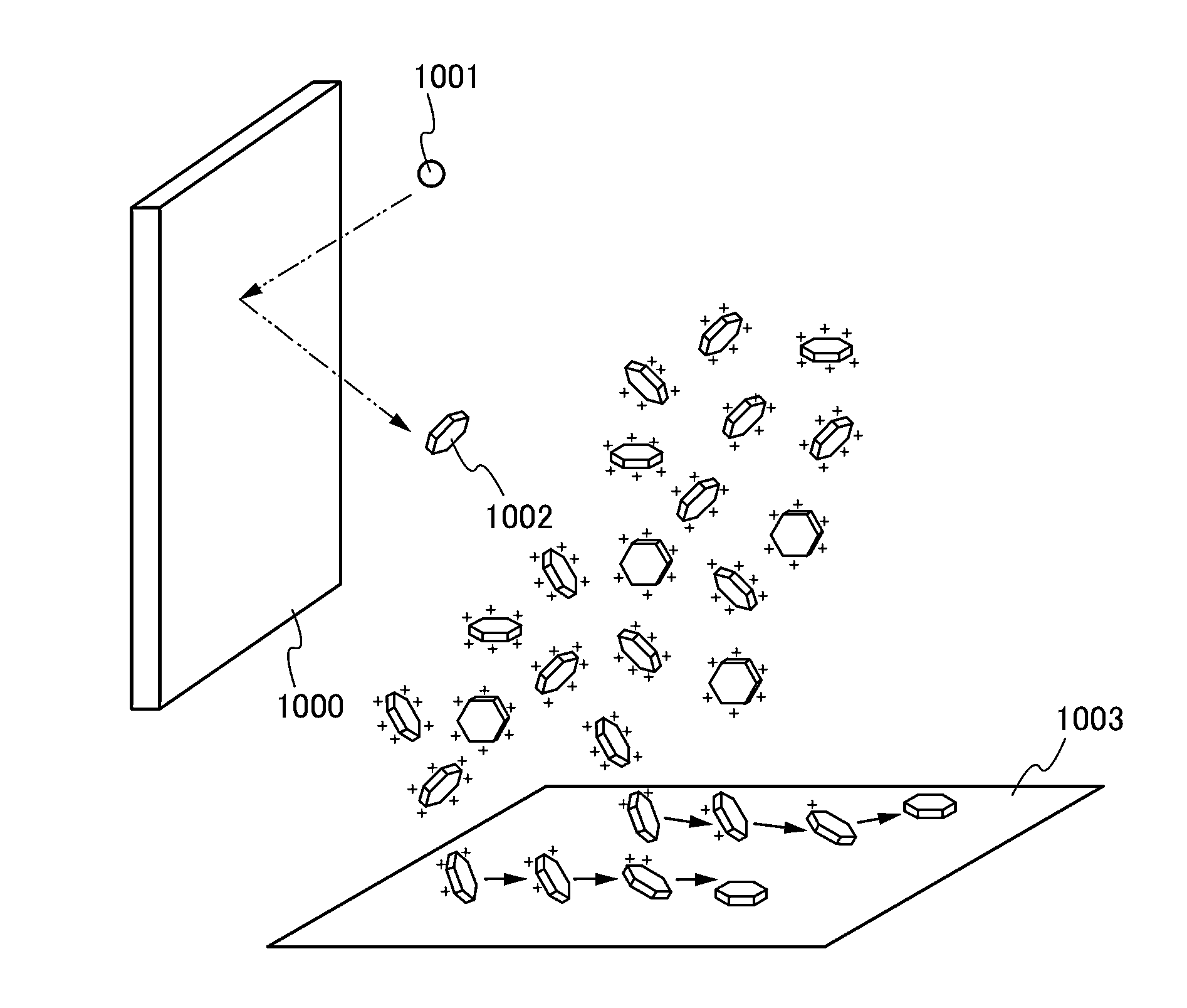
[0190]In this embodiment, a method for using the sputtering target described in Embodiment 1 will be described. In particular, a method for forming an oxide film with a high degree of crystallinity by using the sputtering target described in Embodiment 1 will be described.
[0191]The sputtering target is used by collision of an ion with a surface of the sputtering target.
[0192]As an ion, an oxygen cation is used. Further, in addition to the oxygen cation, an argon cation may be used. Instead of the argon cation, a cation of another rare gas may be used.
[0193]With use of the oxygen cation as the ion, plasma damage at the film formation can be alleviated. Thus, when the ion collides with the surface of the sputtering target, a lowering in crystallinity of the sputtering target can be suppressed or a change of the sputtering target into an amorphous state can be suppressed.
[0194]When the ion collides with the surface of the sputtering target, a crystal grain included in the sputtering ta...
embodiment 3
[0203]In this embodiment, a film formation apparatus with which the oxide film with a high degree of crystallinity described in Embodiment 2 is formed will be described.
[0204]First, a structure of a film formation apparatus which allows the entry of few impurities into a film during film formation is described with reference to FIG. 11 and FIGS. 12A to 12C.
[0205]FIG. 11 is a top view schematically illustrating a single wafer multi-chamber film formation apparatus 4000. The film formation apparatus 4000 includes an atmosphere-side substrate supply chamber 4001 including a cassette port 4101 for holding a substrate and an alignment port 4102 for performing alignment of a substrate, an atmosphere-side substrate transfer chamber 4002 through which a substrate is transferred from the atmosphere-side substrate supply chamber 4001, a load lock chamber 4003a where a substrate is carried and the pressure inside the chamber is switched from atmospheric pressure to reduced pressure or from red...
PUM
| Property | Measurement | Unit |
|---|---|---|
| grain size | aaaaa | aaaaa |
| grain size | aaaaa | aaaaa |
| angle | aaaaa | aaaaa |
Abstract
Description
Claims
Application Information