Method for depositing dielectric films

a technology of dielectric films and substrates, applied in chemical vapor deposition coatings, coatings, metallic material coating processes, etc., can solve the problems of reduced channel mobility, large densities of interface traps, and various problems of current high-k dielectric materials under evaluation, so as to reduce or substantially eliminate the amount of contaminants and improve the control of concentration

Active Publication Date: 2013-12-26
TOKYO ELECTRON LTD
View PDF7 Cites 384 Cited by
  • Summary
  • Abstract
  • Description
  • Claims
  • Application Information

AI Technical Summary

Benefits of technology

[0042]FIG. 1E schematically shows a dielectric film 110 following the exposure of the dielectric film 108 to the hydrogen halide precursor which reduces or substantially eliminates the amount of contaminants 106 in the dielectric film 108. The dielectric film 110 may subsequently further processed to form a semiconductor device.
[0043]The inventors have realized, that the generation of a hydrogen halide gas in the process chamber from a hydrogen ha

Problems solved by technology

Current high-k dielectric materials under evaluation suffer from various problems.
Some of the problems encountered include film crystallization during anneals, growth of interfacial layers during deposition and further processing, large densities of interface traps, reduced channel mobility, reaction w

Method used


Image

  • Method for depositing dielectric films
  • Method for depositing dielectric films
  • Method for depositing dielectric films

Examples


Embodiment Construction

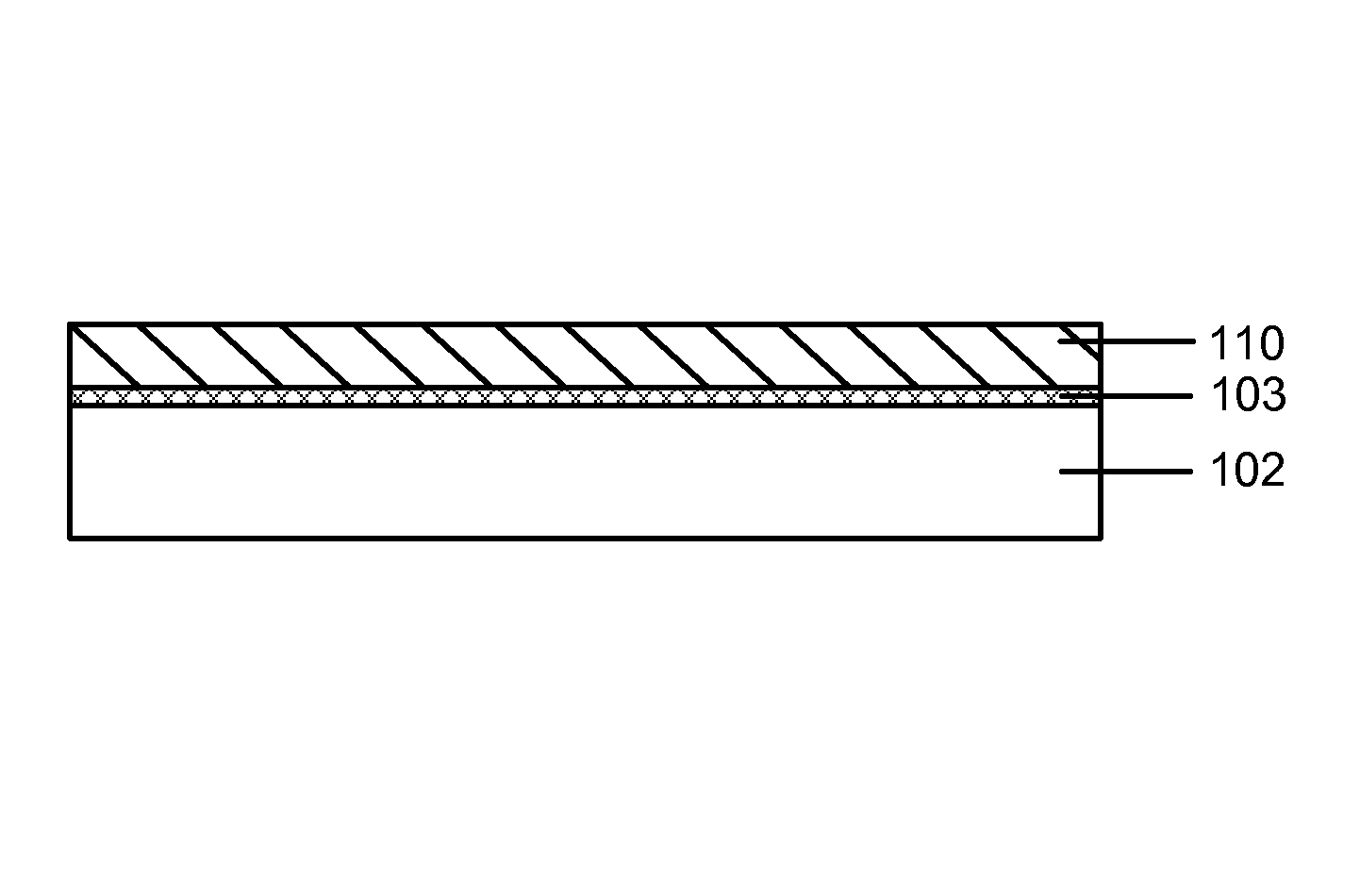
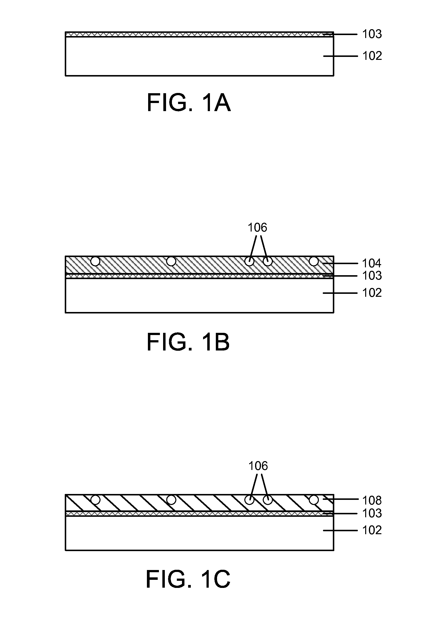
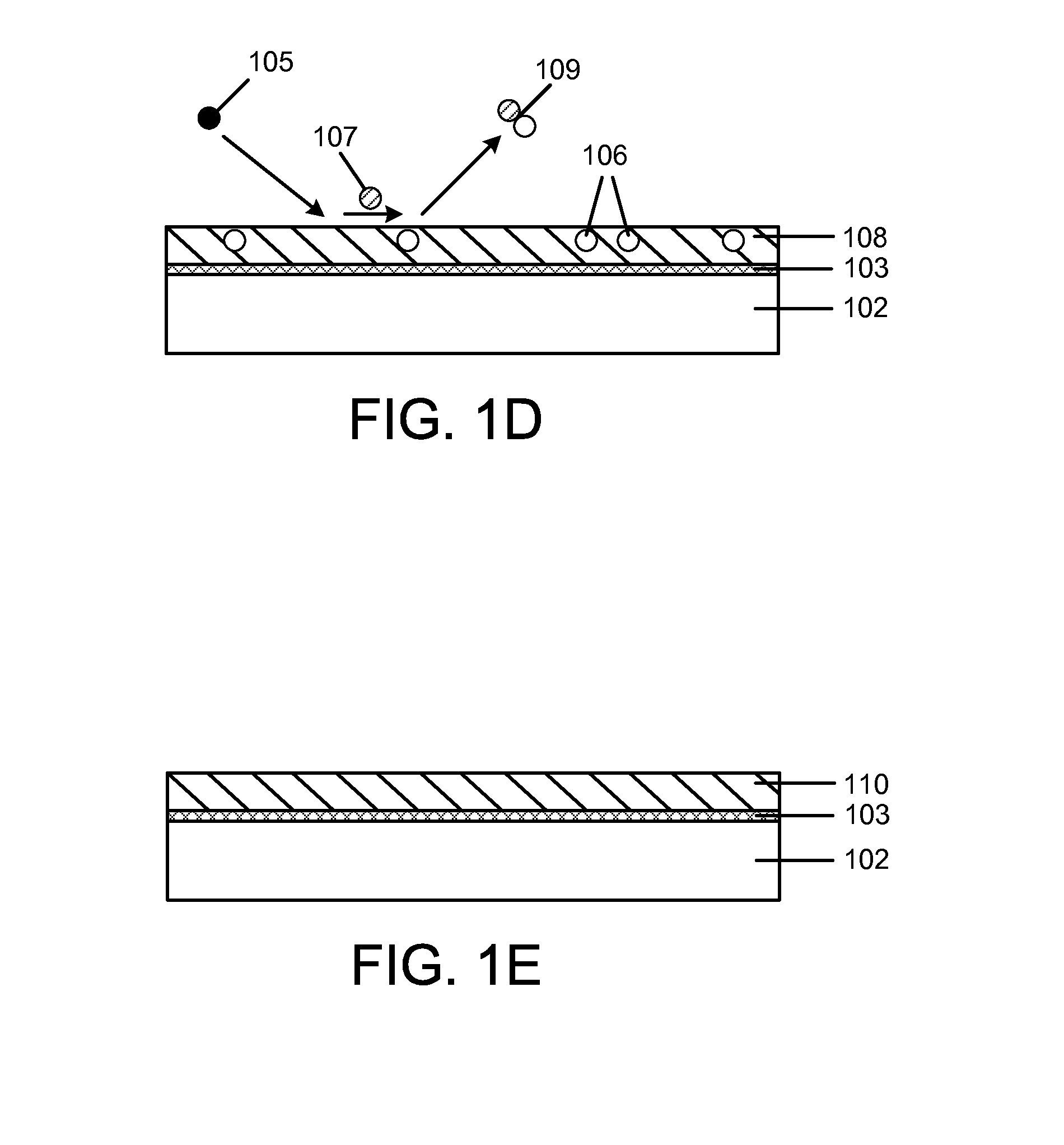
[0018]A method is provided for depositing dielectric films on a substrate. The dielectric films can be conformally deposited using a low thermal budget and provide low leakage current when integrated into a semiconductor device. This is achieved by depositing the dielectric films with low levels of contaminants and defects. According to some embodiments, the dielectric films can include high-dielectric-constant (high-k) films that contain a metal element, for example HfO2 and ZrO2 films. According to another embodiment, the dielectric films can include silicon-containing dielectric films that do not contain a metal element, for example SiO2, SiN, and SiON. According to other embodiments, the dielectric films can include high-k films that contain a metal element and silicon, for example HfSiOx and ZrSiOx.

[0019]Many metal-organic precursors contain contaminants and impurities that can become incorporated into the dielectric films. For example, incorporation of carbon (and / or other con...


PUM


Abstract

A method is provided for depositing a dielectric film on a substrate. According to one embodiment, the method includes providing the substrate in a process chamber, exposing the substrate to a gaseous precursor to form an adsorbed layer on the substrate, exposing the adsorbed layer to an oxygen-containing gas, a nitrogen-containing gas, or an oxygen- and nitrogen-containing gas, or a combination thereof, to form the dielectric film on the substrate, generating a hydrogen halide gas in the process chamber by a decomposition reaction of a hydrogen halide precursor gas, and exposing the dielectric film to the hydrogen halide gas to remove contaminants from the dielectric film.

Description

FIELD OF THE INVENTION[0001]The present invention relates to semiconductor processing, and more particularly, to forming dielectric films on a substrate.BACKGROUND OF THE INVENTION[0002]High dielectric constant (high-k) materials are desirable for use as capacitor dielectrics and for use as gate dielectrics in future generations of electronic devices. The first high-k materials used as capacitor dielectrics were tantalum oxide and aluminum oxide materials. Currently, hafnium aluminum oxide materials are being implemented as capacitor dielectrics in DRAM production. Similarly, hafnium-based dielectrics are expected to enter production as gate dielectrics, thereby replacing or complimenting the current silicon-containing materials.[0003]The most common methods of depositing high-k dielectrics include physical vapor deposition (PVD), chemical vapor deposition (CVD) and atomic layer deposition (ALD). The advantages of using ALD over PVD and CVD methods include improved thickness control...

Claims


Application Information

Patent Timeline
IPC IPC(8): C23C16/455C23C16/34C23C16/40
CPCC23C16/34C23C16/308C23C16/347C23C16/402C23C16/405C23C16/407C23C16/45531C23C16/45534
Inventor CLARK, ROBERT D.
Owner TOKYO ELECTRON LTD
Why Eureka
Try Eureka