Method for Preparing GOI Chip Structure

a chip structure and chip technology, applied in the field of preparing a chip structure, can solve the problems of increasing investment and market risks, unable to continuously improve the performance of silicon-based devices on the basis of an existing very large scale integration (vlsl) technique without significant investment, and the bulk germanium wafer is heavier than the silicon, so as to reduce the effect of reducing the dislocation density of the goi and reducing the temperature of the reaction furna

Active Publication Date: 2014-01-02
SHANGHAI INST OF MICROSYSTEM & INFORMATION TECH CHINESE ACAD OF SCI
View PDF4 Cites 6 Cited by
  • Summary
  • Abstract
  • Description
  • Claims
  • Application Information

AI Technical Summary

Benefits of technology

[0031]2-7): repeating step 2-5) and step 2-6) 4 times, reducing the temperature of the reaction furnace from 900° C. to 600° C. within an hour under the atmosphere of N2, implementing the germanium concentration to form the stacked structure, sequentially comprising the second Si substrate, the insulating buried layer BOX, the Ge layer, and the SiO2 layer.
[0032]As described above, the method for preparing a GOI chip structure of the present invention has the following benefits.
[0033]In the present invention, first, the SGOI chip structure is made out by using the Smart-Cut technique, and then, the germanium concentration is performed on the SGOI chip struct...

Problems solved by technology

With rapid development of silicon-based large scale integrated circuit technologies, performances of bulk silicon complementary metal-oxide-semiconductor (CMOS) devices are gradually approaching physical limits of silicon materials, and the further improving of the performances of the bulk silicon CMOS devices along a direction guided by Moore's Law will face growing investments and market risks.
How to constantly improve the performances of the silicon-based devices on the basis of an existing very large scale integration (VLSL) technique without a significant increase in investment has become a common problem in the industry.
A bulk germanium wafer is heavier than the silicon, and is fragile.
An epitaxy method applied to a germanium donor can easily change the germanium donor...

Method used


Image

  • Method for Preparing GOI Chip Structure
  • Method for Preparing GOI Chip Structure
  • Method for Preparing GOI Chip Structure

Examples


Embodiment Construction

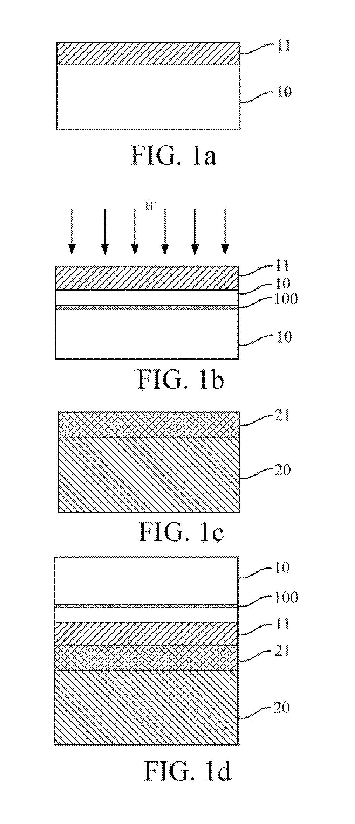
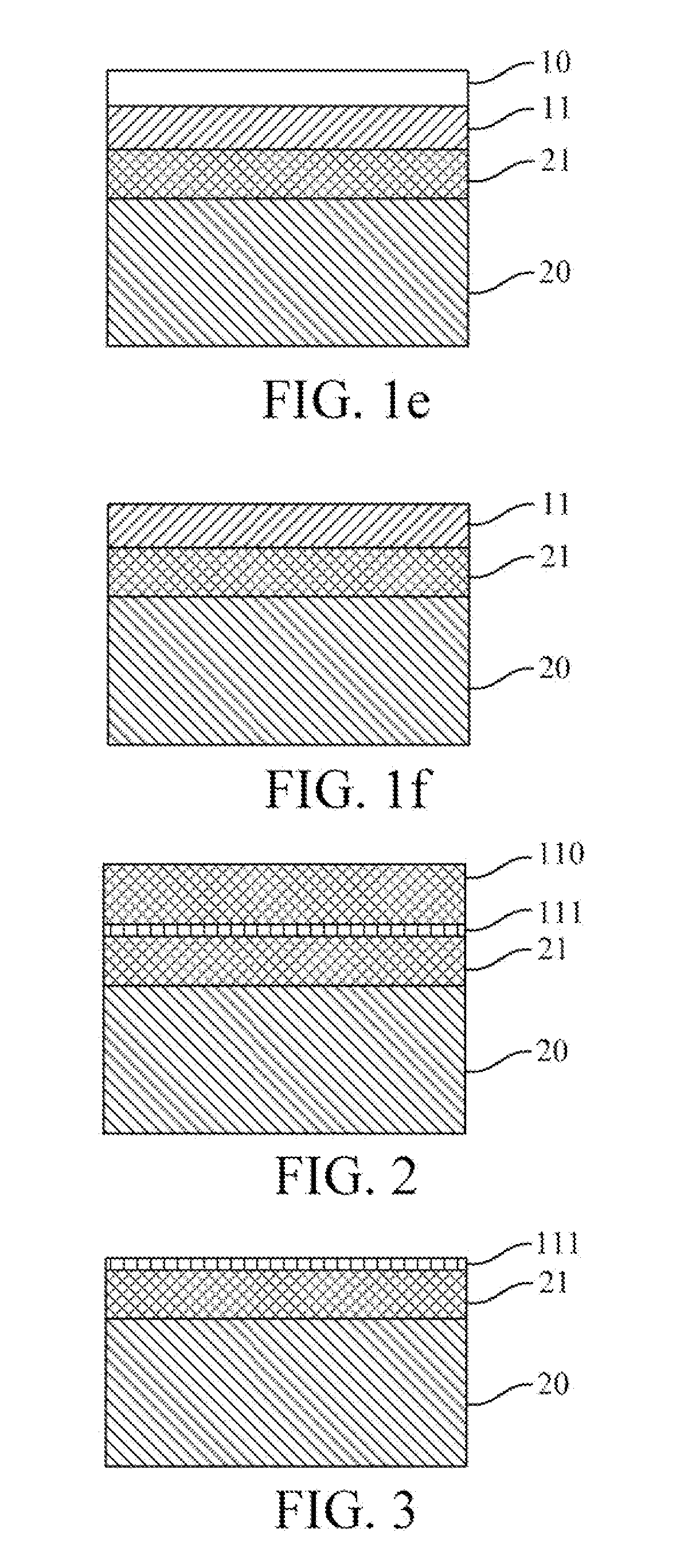
[0043]Implementations of the present invention are described through the specific embodiments below. According to the content disclosed by the specification, persons skilled in the art can easily understand other advantages and effects of the present invention. The present invention can also be implemented or applied through other different specific embodiments. Based on different views and applications, modifications or changes can be made for the details of the specification without departing from the spirit of the present invention.

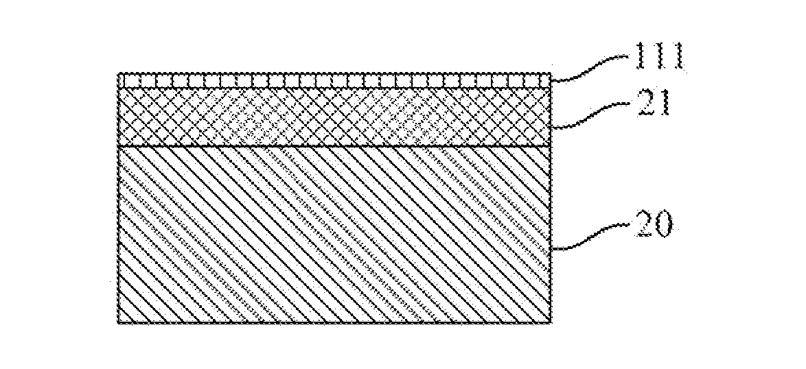
[0044]Referring to FIG. 1a to FIG. 1f, and FIG. 2 to FIG. 3, it should be noted that, only the basic idea of the present invention is schematically illustrated by the drawings provided in this embodiment, so that the drawings merely show the components relevant to the present invention, and are not drawn according to the number, the shapes, and the sizes of the components in actual implementations; the shapes, the number and the ratio of the components...


PUM


Abstract

The present invention provides a method for preparing a GOI chip structure, where, in the method, first, a SiGe on insulator (SGOI) chip structure is made by using a Smart-Cut technology, and then, germanium condensation technology is performed on the SGOI chip structure, so as to obtain a GOI chip structure. Because the SGOI made by the Smart-Cut technology basically has no misfit dislocation in an SGOI/BOX interface, the threading dislocation density of the GOI is finally reduced. A technique of the present invention is simple, the high-quality GOI chip structure can be implemented, and the germanium condensation technology is greatly improved. An ion implantation technology and an annealing technology are quite mature techniques in the current semiconductor industry, so that such a preparation method greatly improves the possibility of wide use of the germanium concentration technology in the semiconductor industry.

Description

BACKGROUND OF THE PRESENT INVENTION[0001]1. Field of Invention[0002]The present invention relates to a method for preparing a chip structure, specifically to a method for preparing a germanium-on-insulator (GOI) chip structure.[0003]2. Description of Related Arts[0004]With rapid development of silicon-based large scale integrated circuit technologies, performances of bulk silicon complementary metal-oxide-semiconductor (CMOS) devices are gradually approaching physical limits of silicon materials, and the further improving of the performances of the bulk silicon CMOS devices along a direction guided by Moore's Law will face growing investments and market risks. The semiconductor industry is a market quite sensitive to a ratio of quality to price of the product. How to constantly improve the performances of the silicon-based devices on the basis of an existing very large scale integration (VLSL) technique without a significant increase in investment has become a common problem in the ...

Claims


Application Information

Patent Timeline
IPC IPC(8): H01L21/762
CPCH01L21/76254
Inventor DI, ZENGFENGYE, LINXUE, ZHONGYINGZHANG, MIAO
Owner SHANGHAI INST OF MICROSYSTEM & INFORMATION TECH CHINESE ACAD OF SCI
Why Eureka
Try Eureka