

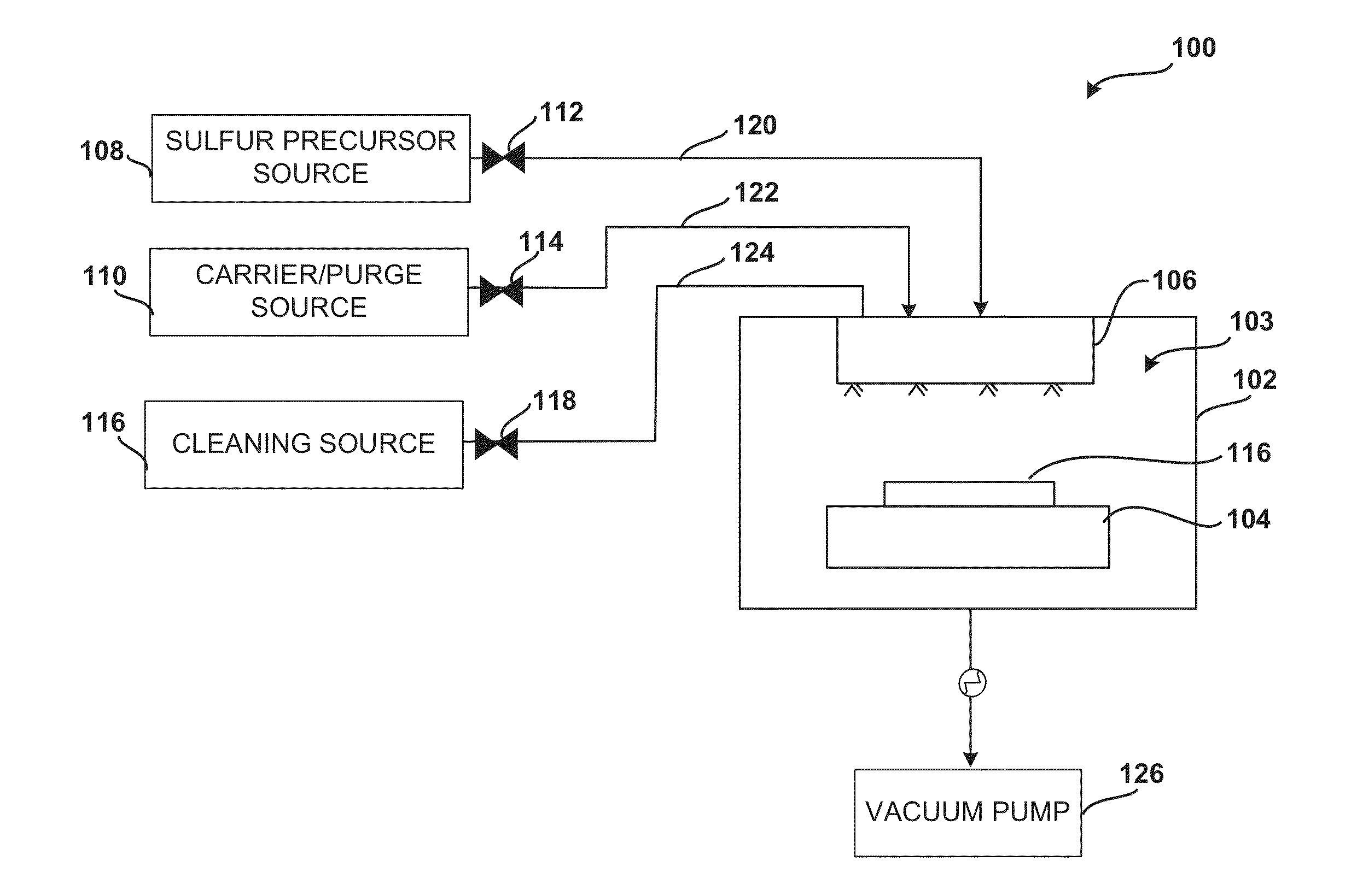
System and method for gas-phase sulfur passivation of a semiconductor surface
a technology of gas-phase sulfur and semiconductors, which is applied in the direction of chemical vapor deposition coating, coating, basic electric elements, etc., can solve the problems of undesired air exposure time, difficult integration of immersion based passivation process into vacuum or gas-phase deposition system used for subsequent dielectric material deposition, and affecting device performance. , to achieve the effect of low dit valu
- Summary
- Abstract
- Description
- Claims
- Application Information
AI Technical Summary
Benefits of technology
Problems solved by technology
Method used
Image

Examples
specific examples
[0039]The following non-limiting examples illustrate a process of passivating a surface of high-mobility semiconductor material and a device or structure formed using the process. These examples are merely illustrative, and it is not intended that the disclosure be limited to the examples.
example 1
[0042]An n-doped In0.53Ga0.47As semiconductor surface was epitaxially grown over a two inch InP substrate. The native oxide on the In0.53Ga0.47As surface was removed using a diluted HCl solution as set forth in the Comparative Example, and the samples were loaded into a reactor chamber within five minutes of completing the clean, to control an amount of time the surface was exposed to ambient air.
[0043]The surface was passivated with sulfur by exposing the surface to a mixture of carrier gas (nitrogen) and a sulfur precursor source (22% (NH4)2S solution source). The reactor chamber temperature was about 300° C., the reaction time about 5 minutes, and the chamber pressure at about 4 Torr.
[0044]An in situ ALD Al2O3 layer was then deposited onto the passivated workpiece surface using TMA and H2O as the precursors, without breaking vacuum between the passivation and dielectric material deposition steps. The thickness of the Al2O3 layer was about 1 nm for XPS analysis and about 5 nm for ...
example 2
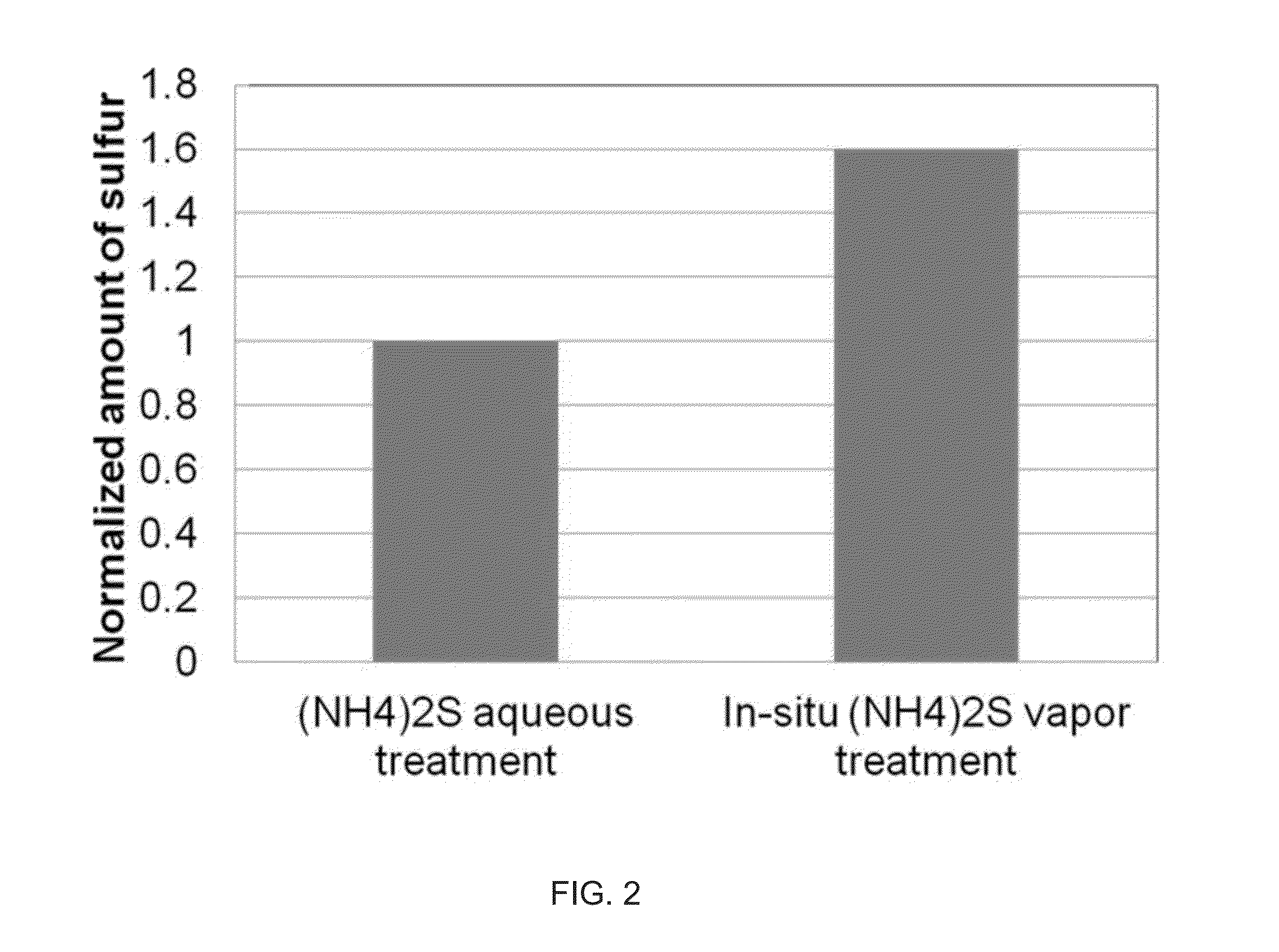
[0047]An n-doped In0.53Ga0.47As semiconductor surface was epitaxially grown over a two inch InP substrate. The native oxide on the In0.53Ga0.47As surface was removed using a diluted HCl solution as set forth in the Example 1. The surface was passivated by ex situ (NH4)2S vapor. An ALD Al2O3 layer was then deposited onto the passivated workpiece surface using TMA and H2O as the precursors. The thickness of the Al2O3 layer was about 1 nm for XPS analysis and about 5 nm for electrical characterization samples. For the samples used for electrical characterization, the dielectric material was then annealed at about 400° C. for about five minutes in a 10% hydrogen in nitrogen environment.
[0048]FIGS. 4(a)-4(c) illustrate improved frequency dispersion capacitance-voltage (C-V) characteristic of the devices formed in accordance with Examples 1 and 2, compared to the Comparative Example and to samples with no passivation. The C-V dispersion measurements were performed over frequencies in the ...
PUM
 Abstract
Description
Claims
Application Information