Scanning signal line drive circuit, display device having the same, and drive method for scanning signal line

a drive circuit and scanning signal technology, applied in the direction of electric digital data processing, instruments, computing, etc., can solve the problem that video signals indicative of pixel voltage values for a plurality of rows cannot be transmitted by each source line at once (simultaneously), and achieve the effect of reducing the stress on the control terminal of the output control switching element, reducing the dullness of the scanning signal as the output signal of the bistable circui

Active Publication Date: 2014-02-06
SHARP KK
View PDF2 Cites 20 Cited by
  • Summary
  • Abstract
  • Description
  • Claims
  • Application Information

AI Technical Summary

Benefits of technology

[0070]According to the first aspect of the present invention, in the control period included in the vertical blanking period, the output control switching element is driven by a voltage lower than that in the conventional technique. Consequently, stress to the control terminal of the output control switching element is reduced as compared with the conventional technique. Thus, the threshold shift in the output control switching element is suppressed, so that dullness of a scanning signal as the output signal of the bistable circuit can be suppressed.
[0071]According to the second aspect of the present invention, in the case of controlling the potential of the first node by the potential of the second node, in a period other than a period for outputting an active output signal, the potential of the second node changes with fluctuation in the second clock signal having the phase opposite to that of the first clock signal. Consequently, in the period other than the period for outputting the active output signal, the potential fluctuation in the first node caused by the potential fluctuation in the first clock signal is suppressed. Therefore, stabilization of the circuit operation can be realized.
[0072]According to the third aspect of the present invention, in the control period included in the vertical blanking period, supply of the clock signal to the bistable circuit is stopped. Consequently, the switching element to be driven by a voltage lower than that in the conventional technique is more reliably driven by a voltage lower than that in the conventional technique.
[0073]According to the fourth aspect of the present invention, in the control period included in the vertical blanking period, the potential of the second node is reliably maintained at the off level. Consequently, the second-node-on-time first node turnoff switching element reliably enters an off state. Thus, since the output control switching element is reliably driven by a voltage lower than that in the conventional technique, stress to the control terminal of the output control switching element is reliably reduced. Therefore, threshold shift in the second-node-on-time first node turn off switching element is reliably suppressed, so that dullness of a scanning signal as the output signal of the bistable circuit can be reliably suppressed.
[0074]According to the fifth aspect of the present invention, the first-clock-signal-on-time second node turn off switching element is driven by a voltage lower than that in the conventional technique. Consequently, stress to the control terminal of the first-clock-signal-on-time second node turn off switching element is reduced as compared with the conventional technique. Thus, since the threshold shift in the first-clock-signal-on-time second node turn off switching element is suppressed, the second-node-on-time first node turn off switching element is controlled more accurately. Therefore, stabilization of the circuit operation can be achieved.
[0075]According to the sixth aspect of the present invention, in the control period included in the vertical blanking period, supply of the first clock signal to the plurality of bistable circuits is stopped, and a terminal in each bistable circuit for receiving the first clock signal enters a high impedance state. Consequently, the first-clock-signal-on-time second node turn off switching element is more reliably driven by a voltage lower than that in the conventional technique. Consequently, stress to the control terminal of the first-clock-signal-on-time second node turn off switching element is more reliably reduced as compared with the conventional technique. Therefore, threshold shift in the first-clock-signal-on-time second node turn off switching element is more reliably suppressed.

Problems solved by technology

However, video signals indicative of pixel voltage values for a plurality of rows cannot be transmitted by each source line at once (simultaneously).

Method used


Image

  • Scanning signal line drive circuit, display device having the same, and drive method for scanning signal line
  • Scanning signal line drive circuit, display device having the same, and drive method for scanning signal line
  • Scanning signal line drive circuit, display device having the same, and drive method for scanning signal line

Examples


first embodiment

1. First Embodiment

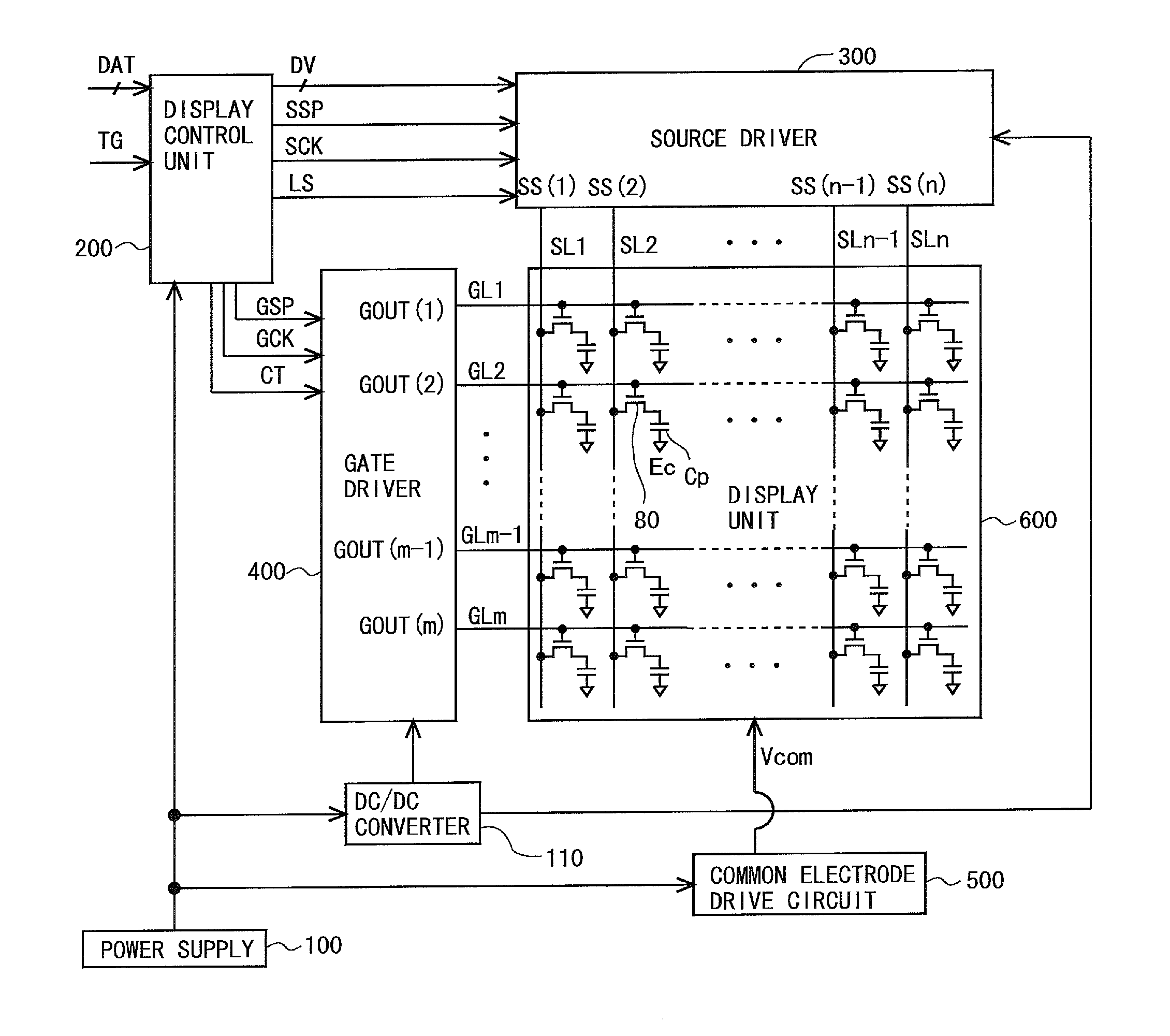
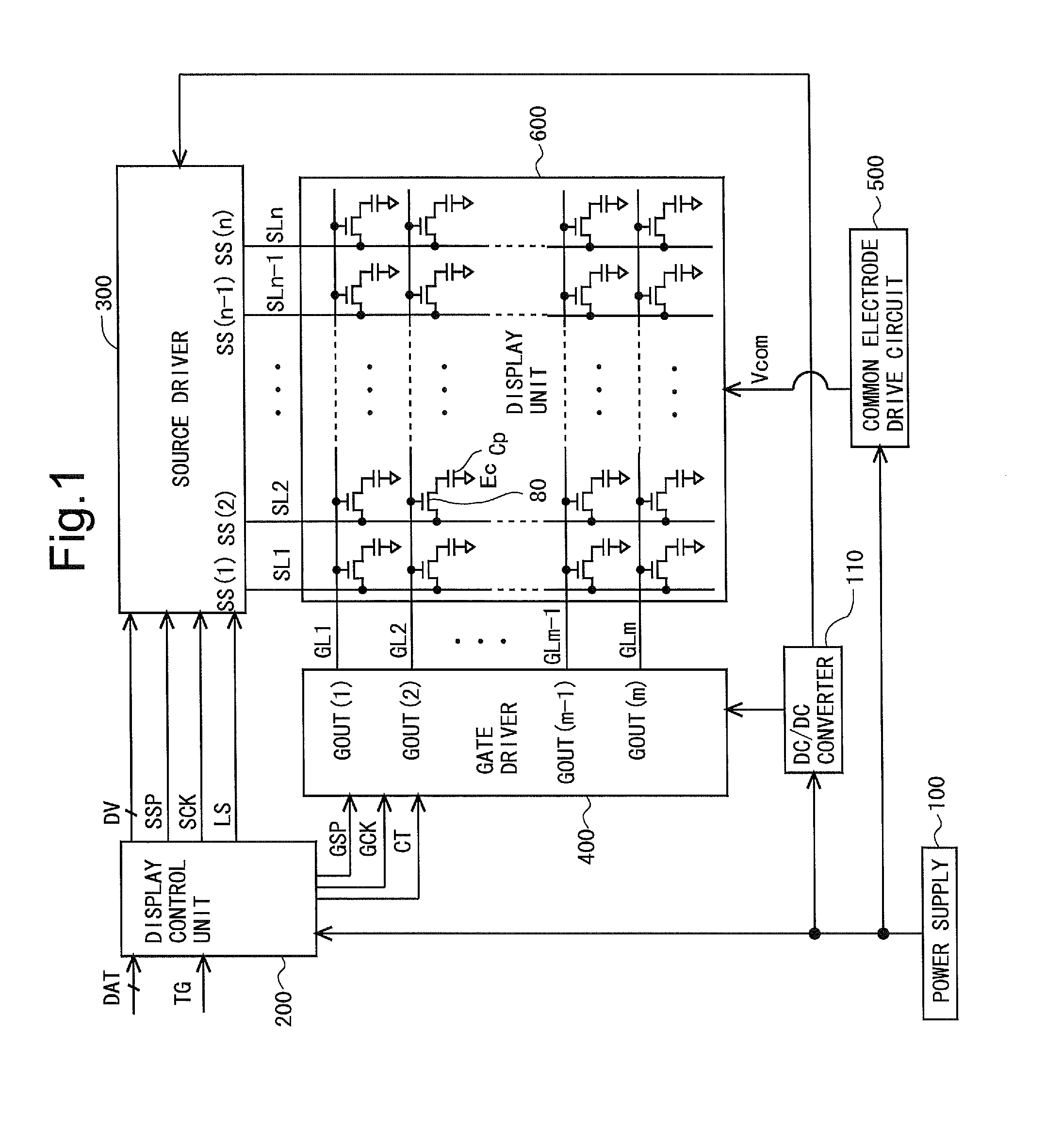
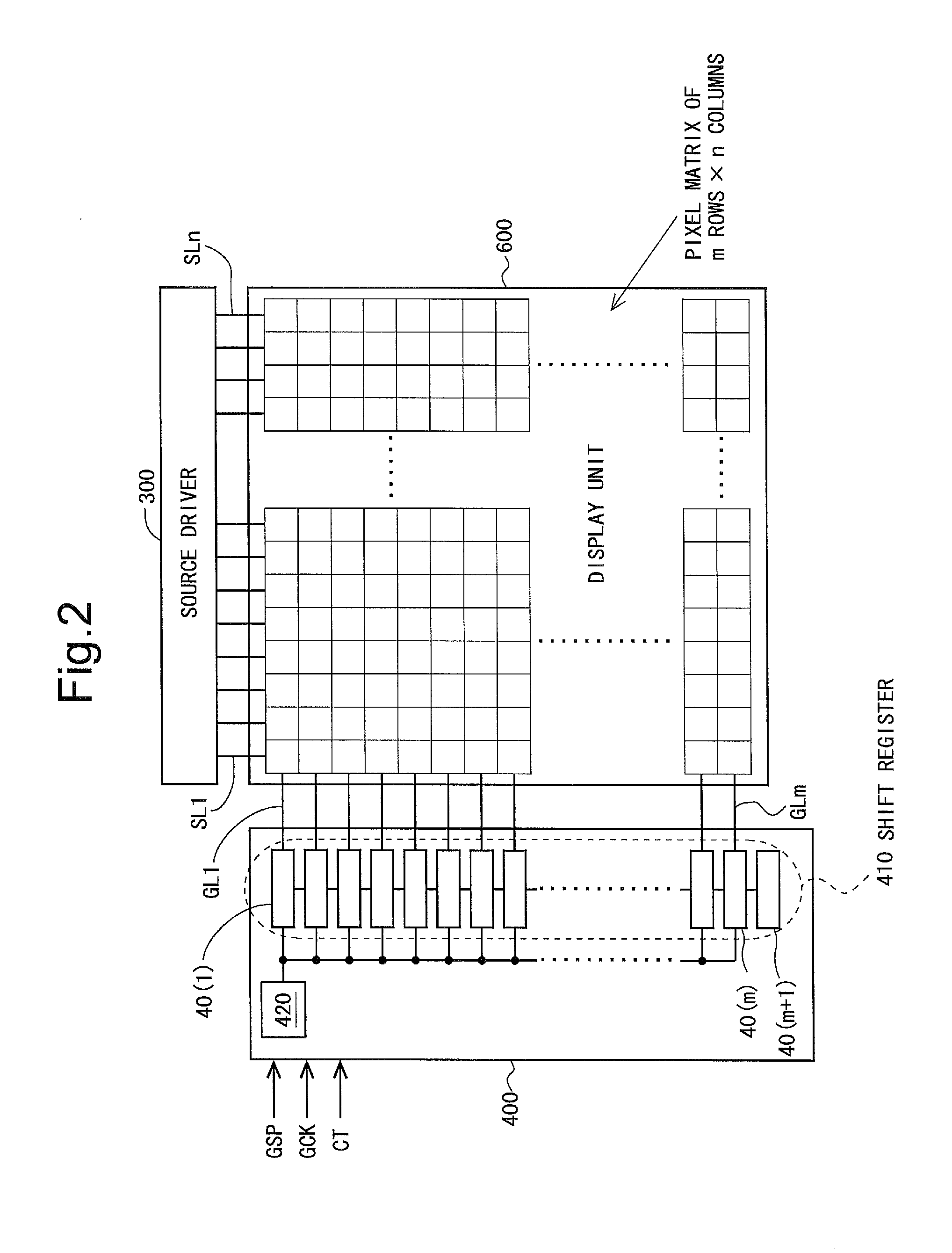
[0104]FIG. 1 is a block diagram illustrating an overall configuration of an active matrix-type liquid crystal display device according to a first embodiment of the present invention. As illustrated in FIG. 1, the liquid crystal display device includes a power supply 100, a DC / DC converter 110, a display control circuit 200, a source driver (a video signal line drive circuit) 300, a gate driver (a scanning signal line drive circuit) 400, a common electrode drive circuit 500, and a display unit 600. It should be noted that the gate driver 400 is formed on a display panel including the display unit 600 by using amorphous silicon, polycrystal silicon, microcrystal silicon, oxide semiconductor (for example, IGZO), or the like. That is, in the present embodiment, the gate driver 400 and the display unit 600 are formed on the same substrate (the array substrate which is one of two substrates constituting the liquid crystal panel). Consequently, the picture-frame area of ...

second embodiment

2. Second Embodiment

[0143]FIG. 13 is a circuit diagram for explaining the configuration of a bistable circuit in a second embodiment of the present invention. Since the general configuration and operation of the liquid crystal display device and the configuration and operation in a write period of the gate driver 400 in the present embodiment are similar to those in the first embodiment, their description is omitted. As illustrated in FIG. 13, a thin film transistor TB is further provided in the bistable circuit in the present embodiment. It should be noted that, since the other configuration is similar to that of the foregoing first embodiment, the description thereof is omitted.

[0144]With respect to the thin film transistor TB, the gate terminal is connected to the input terminal 48, the drain terminal is connected to the gate terminal (input terminal 43) of the thin film transistor T5, and the source terminal is connected to the input terminal 49. When the potential of the contro...

third embodiment

3. Third Embodiment

[0151]FIG. 15 is a circuit diagram for explaining the configuration of a bistable circuit in the third embodiment of the present invention. Since the general configuration and operation of the liquid crystal display device and the configuration and operation in a write period of the gate driver 400 in the present embodiment are similar to those in the first embodiment, their description are omitted. As illustrated in FIG. 15, a thin film transistor TC is further provided in the bistable circuit in the present embodiment.

[0152]With respect to the thin film transistor TC, the gate terminal is connected to the input terminal 48, the drain terminal is connected to the gate terminal and the drain terminal (input terminal 44) of the thin film transistor T3, and the source terminal is connected to the input terminal 49. When the potential of the control signal CT is at the high level, the thin film transistor TC changes the potential of the gate terminal and the drain te...


PUM


Abstract

The present invention is directed to suppress dullness of a scanning signal in a scanning signal line drive circuit. A bistable circuit is provided with an input terminal (43) for receiving a first clock signal (CK), an input terminal (48) for receiving a control signal (CT), an input terminal (49) for receiving a level down signal (LD), an output terminal (51), a thin film transistor (T2), and a thin film transistor (TA). The thin film transistor (T2) has a gate terminal connected to a first node (N1), a drain terminal connected to the input terminal (43), and a source terminal connected to the output terminal (51). The thin film transistor (TA) has a gate terminal connected to the input terminal (48), a drain terminal connected to the first node (N1), and a source terminal connected to the input terminal (49). The potential of the control signal (CT) becomes the high level in a control period as a period except for the first one horizontal scanning period in a vertical blanking period. The level down signal (LD) is a potential lower than DC power supply potential (Vss).

Description

TECHNICAL FIELD[0001]The present invention relates to a scanning signal line drive circuit, a display device having the same, and a drive method for a scanning signal line and, more particularly, to a scanning signal line drive circuit suitable for monolithic fabrication, a display device having the same, and a drive method for a scanning signal line by the scanning signal line drive circuit.BACKGROUND ART[0002]Conventionally, a gate driver (a scanning signal line drive circuit) for driving gate lines (scanning signal lines) of a liquid crystal display device is often mounted as an IC (Integrated Circuit) chip in a peripheral portion of a substrate serving as a component of a liquid crystal panel. In recent years, however, formation of a gate driver directly formed on a substrate is gradually increasing. Such a gate driver is called a “monolithic gate driver” or the like.[0003]In a liquid crystal display device having a monolithic gate driver, a thin film transistor using amorphous ...

Claims


Application Information

Patent Timeline
Patent Type & Authority Applications(United States)
IPC IPC(8): G09G3/02
CPCG09G3/02G09G3/20G09G3/36G09G3/3674G09G3/3677
Inventor TANAKA, SHINYA
Owner SHARP KK
Why Eureka
Try Eureka