Defect detection method

a detection method and technology of defect, applied in the direction of optical radiation measurement, instruments, spectrometry/spectrophotometry/monochromators, etc., can solve the problems of reducing the yield, reducing the yield of semiconductor devices, and requiring a large manufacturing cost for lsi manufacturing, so as to achieve high inspection accuracy and increase productivity

Active Publication Date: 2014-02-27
NUFLARE TECH INC
View PDF5 Cites 21 Cited by
  • Summary
  • Abstract
  • Description
  • Claims
  • Application Information

AI Technical Summary

Benefits of technology

[0007]In the nanoimprint technology, to increase productivity, duplicate templates (replica templates) are produced using a master template as an original plate, and the replica templates are used in different nanoimprint apparatuses during forming the fine circuit pattern on the resist. The replica template is required to be produced accurately corresponding to the master template. Thus, high inspection accuracy is required for not only the master template but also the replica template.

Problems solved by technology

Enhancement of yield is essential, as the manufacture of LSI requires a large manufacturing cost.
In these circumstances, a pattern defect of the mask constitutes a major cause of reduction in the yield of the semiconductor device.
In these circumstances, the pattern defect of the mask and variation of process terms and conditions at the time of exposure and transfer constitute a major cause of reduction in the yield.
However, these days, as the circuit pattern size is being decreased, the pattern size is becoming smaller than the resolution of an optical system of an inspection apparatus used in the detection of a defect.
Thus, although an EB (Electron Beam) source is used, throughput is low, and a problem arises in that the source cannot be mass-produced.

Method used


Image

  • Defect detection method
  • Defect detection method
  • Defect detection method

Examples


Embodiment Construction

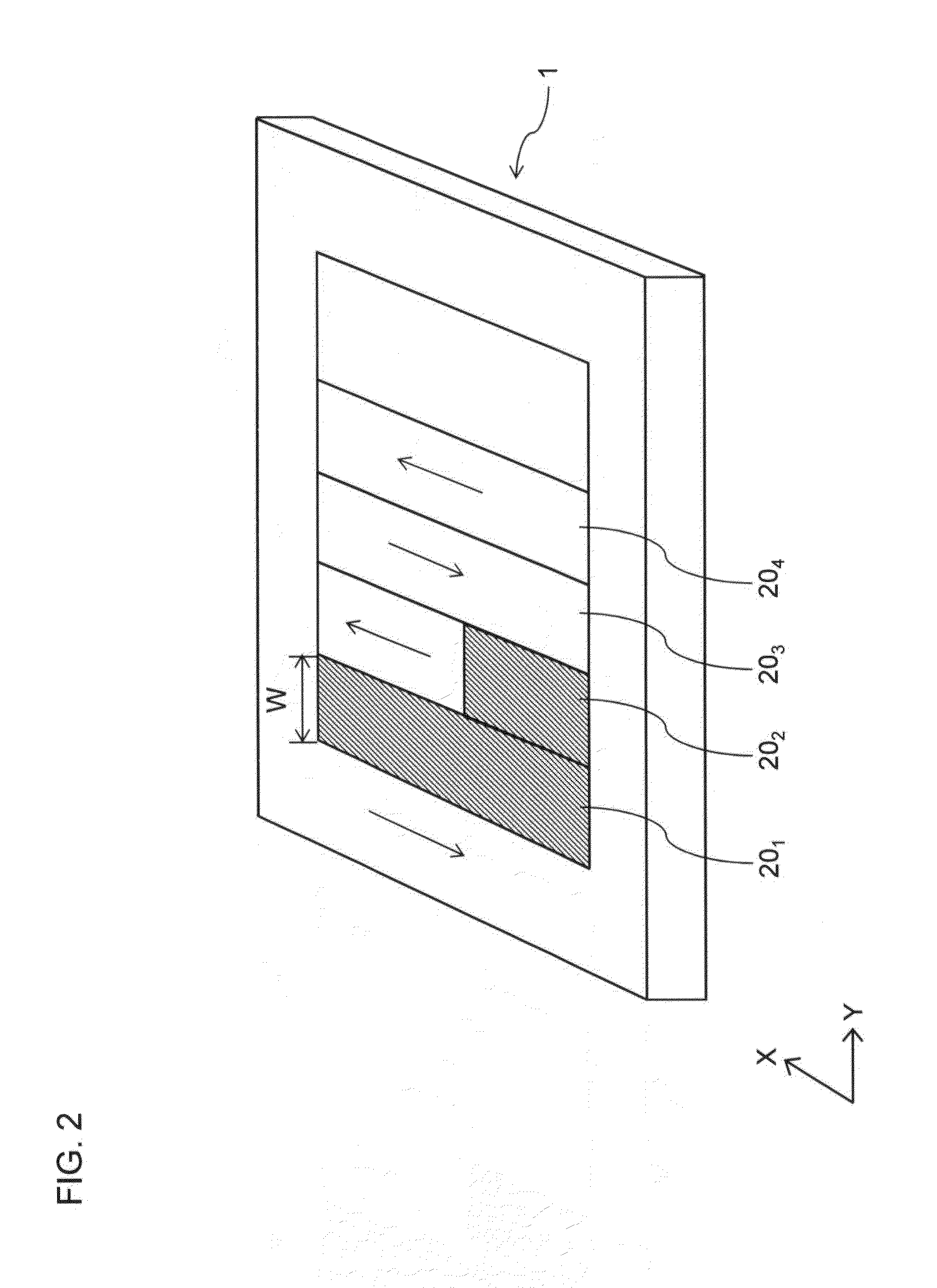
[0028]Many of the patterns formed on a wafer are repeated patterns such as line-and-space patterns, that is, a regular pattern repeated with a periodicity. Accordingly, such repeated patterns are formed on a template used in nanoimprint lithography.

[0029]When a dense pattern image whose line width is smaller than about 100 nm is to be formed by an optical system using DUV light, even if a lens (numerical aperture NA=1) of theoretical limitation is used, this fine pattern cannot be resolved. However, when such a pattern is the repeated pattern, if line edge roughness increases in a part of the pattern, or if a part of the pattern is lacking, the regularity is disturbed to change a tone of an optical image in the part of the pattern, and therefore, the increase of the line edge roughness and the lack of a part of the pattern can be detected as defects.

[0030]However, even if line edge roughness that will not be a defect fluctuates the gray scale value, there is a problem that the fluct...


PUM

PropertyMeasurementUnit
widthaaaaaaaaaa
widthaaaaaaaaaa
defect detectionaaaaaaaaaa

Abstract

A defect detection method comprising, irradiating light from a light source in an optical system and obtaining a plurality of optical images of a sample having a repeated pattern of a size smaller than a resolution of the optical system; while changing the conditions of the optical system, performing correction processing for the optical images with the use of at least one of a noise filter and a convolution filter; shifting a position of the other optical images based on any of the plurality of optical images, obtaining a relationship between shift amounts of the other optical images and a change of correlation of a gray scale value between the plurality of optical images, and performing positional alignment of the optical images based on the shift amount obtained when the correlation is highest, performing defect detection of the sample with the use of the optical images after the positional alignment.

Description

CROSS-REFERENCE TO THE RELATED APPLICATION[0001]The entire disclosure of the Japanese Patent Application No. 2012-184034, filed on Aug. 23, 2012 including specification, claims, drawings, and summary, on which the convention priority of the present application is based, are incorporated herein in its entirety.FIELD OF THE INVENTION[0002]This invention relates to a defect detection method.BACKGROUND[0003]In a large scale integration circuit (LSI), as the degree of integration and the capacity are increased, the circuit size required for a semiconductor device has been gradually decreasing. For example, the most advanced devices require a line width of a few ten nm.[0004]Enhancement of yield is essential, as the manufacture of LSI requires a large manufacturing cost. In the manufacture of the semiconductor device, a pattern is exposed and transferred onto a resist film formed on a wafer by a reduced projection exposure apparatus generally called a stepper or scanner to form a circuit ...

Claims


Application Information

Patent Timeline
Patent Type & Authority Applications(United States)
IPC IPC(8): G01N21/956
CPCG01N21/95623G01N21/9501G01B11/30G01N21/956
Inventor SUGIHARA, SHINJIOGAWA, RIKIINOUE, HIROMU
Owner NUFLARE TECH INC
Why Eureka
Try Eureka