Apparatus for the Automated Testing and Validation of Electronic Components

a technology for electronic components and automatic testing, applied in the direction of electronic circuit testing, measurement devices, instruments, etc., can solve the problems of not being able to meet the speed of assembly speed, the conventional automatic test equipment used to test individual components is limited to less than 12 ghz, and the adoption of higher processing speed is subject to major constraints

Active Publication Date: 2014-03-06
UNIVERSITY OF WINDSOR
View PDF35 Cites 19 Cited by
  • Summary
  • Abstract
  • Description
  • Claims
  • Application Information

AI Technical Summary

Benefits of technology

[0011]In another embodiment, the present invention provides a mounting table test interface module based on MEMS technology, and which is adapted for electronic coupling with a receiver module of an ATE. In a preferred construction, high-speed micro test-channels are provided in the test interface module to establish signal connectivity between the components or unit under test and the tester at the die level, and more preferably which maintain the signal integrity up to 50 GHz without significant signal loss distortion.
[0012]In another embodiment, the present invention provides a MEMS based interface module for use in an ATE to perform high-speed testing of a plurality of electronic components and more preferably such components at a die level, as for example as part of a bulk testing procedure. The provided architecture of the interface module reduces the distance between the unit under test and pin electronics of the ATE less then 2000 and preferably less than about a few hundred micrometers. As a result, the transmission line effects may significantly attenuated, allowing the test channels to operate up to 50 GHz without considerable signal integrity degradation.

Problems solved by technology

Conventional automatic test equipment used to test individual components however, currently experience difficulties keeping pace with faster assembly speeds.
In particular, conventional automatic test equipment (ATE) is limited to less than 12 GHz, and most typically operates at about 4 GHz.
However, major constraints exist with adopting higher processing speeds, as a result of limitations on current mass interconnect system mounting tables.
At frequencies above a few gigahertz, testing integrated circuits becomes a challenging task.
In particular, signal integrity degradation due to parasitic effects of interconnects and electromagnetic coupling undermines the test results at high speeds.
As a result, general purpose pin electronics are commonly bulky and cannot be readily integrated and positioned adjacent to the unit under test pins.
Furthermore, conventional mounting tables consume considerable amounts of power, and in some cases require liquid cooling systems to avoid overheating and maintain desired temperature.
Heretofore, the problem of physical separation between unit under test and pin electronics has not been decisively solved.
Although designing a pin electronics board in such a manner reduces the total length between the unit under test outputs and comparators inputs to approximately 2 to 3 inches for a conventionally packaged VLSI device, a 2 to 3 inch gap may still undermine signal integrity when frequencies exceed a few gigahertz.
While such changes allow the characteristics of the inputs and outputs of the test system to be matched to the component or unit under test I / O pad and reduce both the effects of signal reflection as well as the distance between the device under test and pin electronics, such approach restricts the flexibility of the general purpose pin electronics architecture.
It has been recognized that when the frequency of interaction between the unit under test and the automatic test equipment approaches the gigahertz range, the effects of transmission lines become a critical issue requiring matching impedances to minimize signal reflection and enhance the performance parameters of test channels.
Moreover, AC resistance due to the skin effect and electromagnetic coupling caused by radiation become significant, degrading the signal integrity.
These undesired effects eventually undermine the timing measurement accuracy and the test results.

Method used


Image

  • Apparatus for the Automated Testing and Validation of Electronic Components
  • Apparatus for the Automated Testing and Validation of Electronic Components
  • Apparatus for the Automated Testing and Validation of Electronic Components

Examples


Embodiment Construction

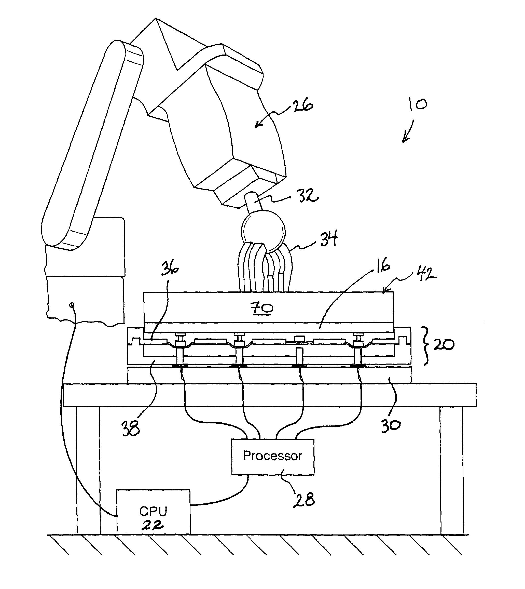
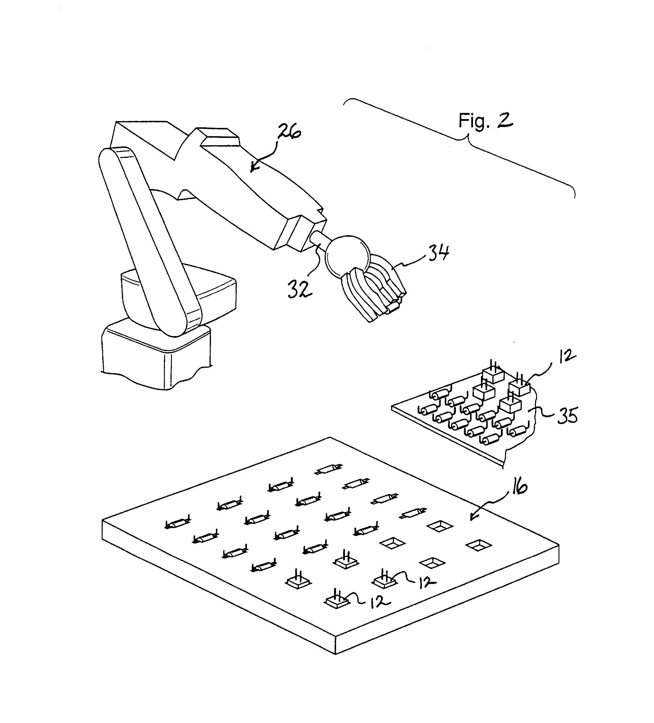
[0030]Reference is made to FIG. 1 which shows an automatic test equipment 10 unit for use in the automated testing and validation of electronic components 12 (FIG. 2) and preferably the concurrent testing of multiple components 12 positioned with a test die 16 prior to their assembly as part of a circuit board and / or the like. As will be described, the automatic test equipment 10 is provided with a mass interconnect system 20 which is configured to achieve the simultaneous high speed testing of a variety of different types of electronic components 12, including by way of non-limiting example, switches, chips, resistors, diodes, and the like without requiring significant device-specific customization and / or reconfiguration for each different die or unit under test 16 to be tested.

[0031]As shown best in FIG. 1, in addition to the mass interconnect system 20, the automatic test equipment 10 includes a main processor 22, a robotic handler assembly 26, a test protocol controller 28, and ...


PUM


Abstract

An automatic test equipment (ATE) unit, which incorporates a mass interconnect system. The mass interconnect system is provided with a universal mounting table for use with receiver and test interface modules for electronically mounting and testing a variety of different types of electronic components or unit under test thereon. The mounting table test interface module incorporates MEMS based spring contacts to provide high-speed micro test-channels in order to establish signal connectivity between the components or unit under test and the tester, and which maintain the signal integrity up to 50 GHz without significant signal loss distortion.

Description

RELATED APPLICATIONS[0001]This application claims the benefit under 35 USC §119(e) to U.S. Provisional Application No. 61 / 457404, filed 21 Mar. 2011, entitled MEMS Based Device Interface Module.SCOPE OF THE INVENTION[0002]The present invention provides an apparatus for the automated testing and validation of electronic components. More particularly, the present invention relates to an apparatus which includes a MEMS based device interface module, and more particularly a high speed test interface panel or module for testing electronic components such as chips, resistors and / or diodes used in electronic circuitry and the like.BACKGROUND OF THE INVENTION[0003]Currently almost 100% of all electronic components are tested prior to assembly onto circuit boards. Such testing is highly desirable as in circuit board assembly processes up to 80,000 components may be used in each assembly line per minute. If a single component is defective, it is typically more cost effective to scrap the enti...

Claims


Application Information

Patent Timeline
Patent Type & Authority Applications(United States)
IPC IPC(8): G01R1/04
CPCG01R1/0408G01R1/06716G01R31/2822G01R31/2889G01R1/073G01R31/28
Inventor RASHIDZADEH, RASHIDAHMADI, MAJIDKANDALAFT, NABEEH
Owner UNIVERSITY OF WINDSOR
Why Eureka
Try Eureka