Semiconductor device

a technology of semiconductor elements and semiconductor components, applied in the field of semiconductor devices, can solve the problems of not being able to fully support the higher current that has been demanded, cannot be applied to the case of a semiconductor, and cannot be fully supported by the higher current, so as to reduce the size of the semiconductor element, and achieve the effect of efficient realization of the wiring substra

Active Publication Date: 2014-03-13
MURATA MFG CO LTD
View PDF14 Cites 15 Cited by
  • Summary
  • Abstract
  • Description
  • Claims
  • Application Information

AI Technical Summary

Benefits of technology

[0026]Heat from the semiconductor element is substantially dissipated from the heat dissipating substrate and is less likely to be transferred to the wiring substrate. Also, the wiring substrate has a thermal conductivity lower than that of the heat dissipating substrate. Thus, since there is no significant increase in temperature on the outer surface of the wiring substrate, a heat-sensitive electronic component can be mounted on the outer surface of the wiring substrate without problems.
[0027]In a preferred embodiment of the present invention, if the wiring substrate includes a through hole passing therethrough in a direction perpendicular or substantially perpendicular to the direction of the principal surface, and the semiconductor element is disposed in the through hole, the entire region around the through hole in the wiring substrate can be used as wiring for the semiconductor element, so that efficient wiring can be realized in the wiring substrate. Additionally, since a space beside the semiconductor element can be effectively used, it is possible to reduce the size of the semiconductor element.
[0028]In the case described above, if there are a plurality of semiconductor elements and a plurality of through holes, and the plurality of semiconductor elements are disposed in the respective through holes, wiring between the plurality of semiconductor element...

Problems solved by technology

However, the technique described in Japanese Unexamined Patent Application Publication No. 61-212045 cannot be applied to the case where a semiconductor element to be mounted is, for example, a field-effect transistor (FET) that requires input and output of signals through its lower surface.
However, the technique described in Japanese Unexamined Patent Application Publication No. 5-315467 cannot fully support higher current that has been demanded in recent years.
An FET that has been recently developed using SiC or GaN semiconductor has a heat resistance temperature as high as 300° C. or 500° C. Although high current can be supplied in this case, the technique described in Japanese Unexamined Patent Application Publication No. 5-315467 cannot fully support such high current.
However, metal having a relative...

Method used


Image

  • Semiconductor device
  • Semiconductor device
  • Semiconductor device

Examples


Embodiment Construction

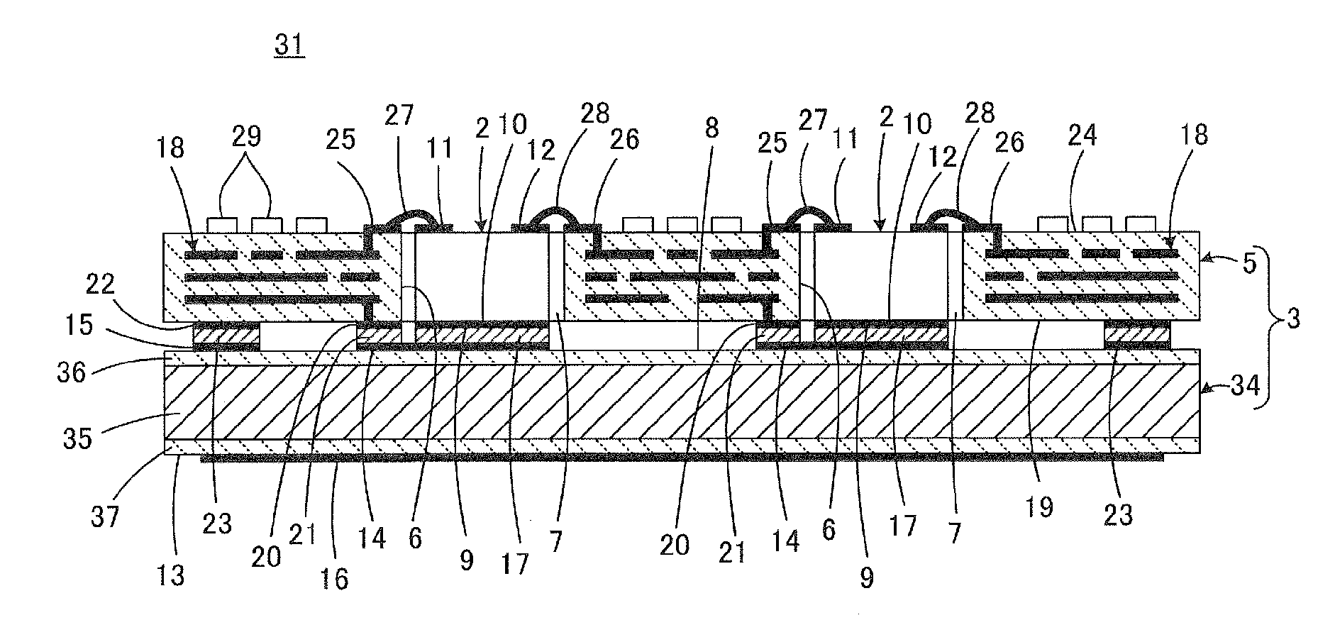
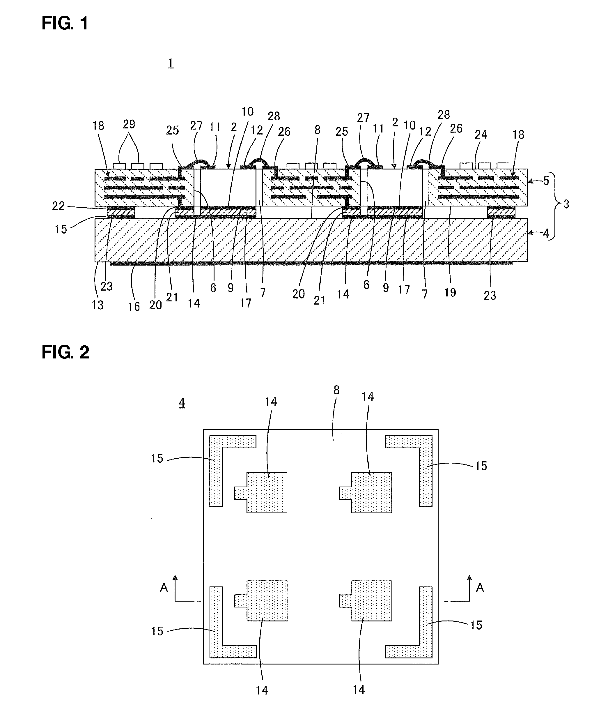
[0038]A semiconductor device 1 according to a first preferred embodiment of the present invention will now be described with reference to FIG. 1 to FIG. 4. FIG. 1 is an enlarged view as compared to FIG. 2 to FIG. 4. The cross section illustrated in FIG. 1 corresponds to a cross section taken along line A-A in FIG. 2.

[0039]As illustrated in FIG. 1, a semiconductor device 1 includes a plurality of semiconductor elements 2 and a substrate assembly 3 to mount the semiconductor elements 2. The substrate assembly 3 is an integrated combination of a heat dissipating substrate 4 and a wiring substrate 5.

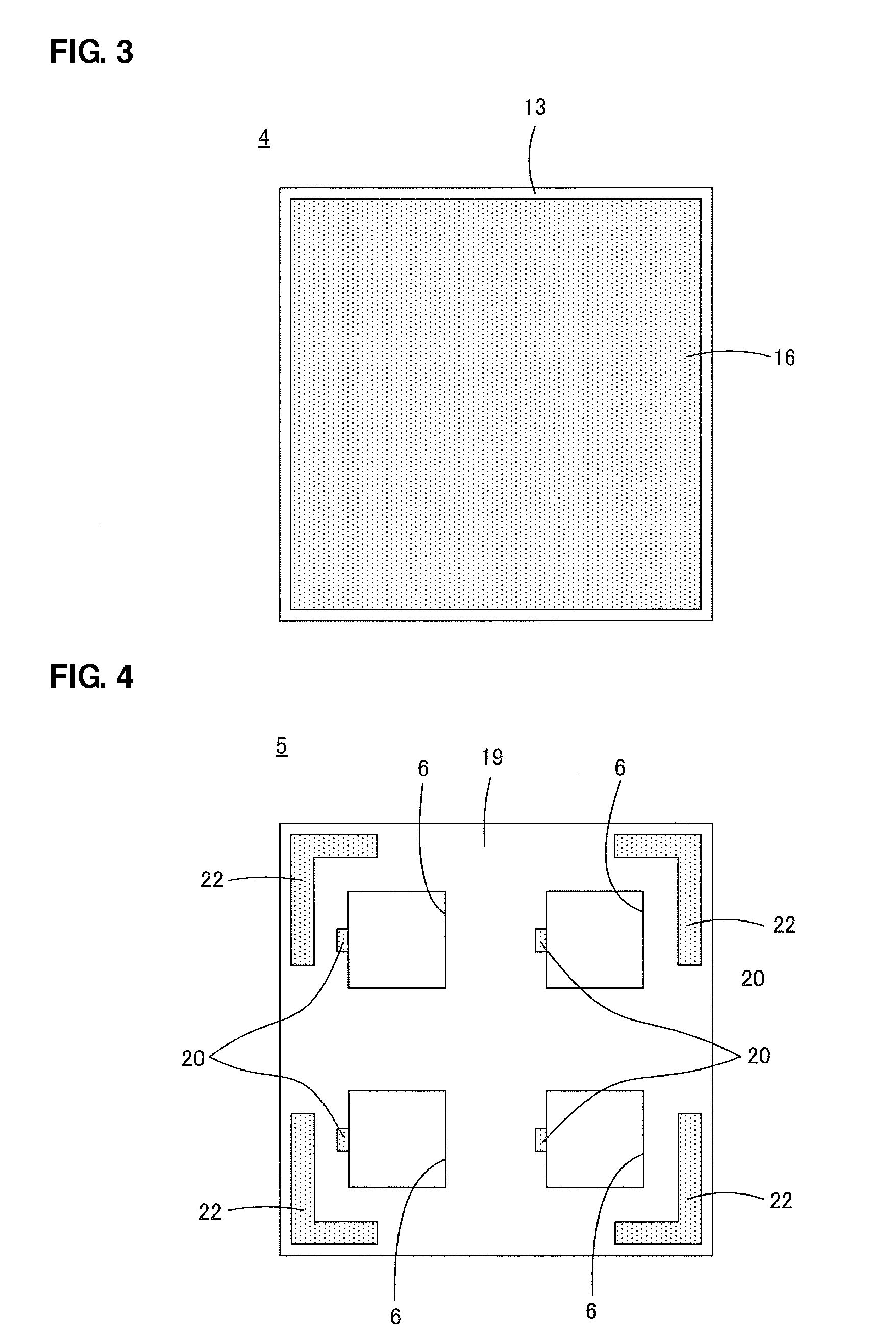
[0040]The wiring substrate 5 includes a plurality of through holes 6 passing therethrough in a direction perpendicular or substantially perpendicular to the principal surface direction. The semiconductor elements 2 described above are disposed in the respective through holes 6. In the illustrated present preferred embodiment, as can been seen from FIG. 4, the wiring substrate 5 preferably in...


PUM


Abstract

In a semiconductor device including a semiconductor element that produces heat and a substrate on which the semiconductor element is mounted, functions of the substrate are divided between a heat dissipating substrate and a wiring substrate. The heat dissipating substrate has a relatively high thermal conductivity, and includes principal surfaces defined by electric insulators, one of which is provided with an outer conductor located thereon. The wiring substrate is mounted on the upper principal surface of the heat dissipating substrate, has a thermal conductivity lower than that of the heat dissipating substrate, and includes a wiring conductor made mainly of silver or copper and located inside the wiring substrate, the wiring conductor being electrically connected to the outer conductor. The semiconductor element is mounted on the upper principal surface of the heat dissipating substrate and disposed in a through hole of the wiring substrate.

Description

BACKGROUND OF THE INVENTION[0001]1. Field of the Invention[0002]The present invention relates to a semiconductor device, and particularly to a semiconductor device that includes a semiconductor element that produces heat during operation and a substrate including the semiconductor element mounted thereon.[0003]2. Description of the Related Art[0004]To efficiently allow heat produced by a semiconductor element included in a semiconductor device to escape, a substrate of low thermal resistance is used as a substrate for mounting the semiconductor element thereon. Examples of the substrate of low thermal resistance currently in practical use include a metal base substrate formed by a metal plate of high thermal conductivity, and high temperature co-fired ceramic (HTCC) substrates, such as an aluminum nitride substrate and an alumina substrate.[0005]For example, Japanese Unexamined Patent Application Publication No. 61-212045 describes a technique in which a ceramic multilayer wiring su...

Claims


Application Information

Patent Timeline
IPC IPC(8): H01L23/34
CPCH01L23/34H01L23/3735H01L23/5383H01L23/5389H01L25/072H01L25/16H01L2224/48157H01L2224/73265H01L2924/09701H01L24/48H01L2924/01019H01L2224/48227H01L2224/32225H01L24/06H01L24/32H01L2224/48101H01L24/73H01L2924/00014H01L2924/00012H01L2224/45099H01L2224/45015H01L2924/207
Inventor MORIYA, YOICHIKANAMORI, TETSUOYAGI, YUKIHIROSUGIMOTO, YASUTAKATAKADA, TAKAHIRO
Owner MURATA MFG CO LTD
Why Eureka
Try Eureka