Transistor device and fabrication method

a technology of transistors and fabrication methods, applied in the field of semiconductor technology, can solve problems such as hot carrier effects, time-related voltage breakdowns, and various problems, and achieve the effects of reducing the number of transistors, and improving the efficiency of transistors

Active Publication Date: 2014-03-20
SEMICON MFG INT (SHANGHAI) CORP
View PDF3 Cites 41 Cited by
  • Summary
  • Abstract
  • Description
  • Claims
  • Application Information

AI Technical Summary

Benefits of technology

[0006]According to various embodiments, there is provided a method for forming a transistor. In this method, a dummy gate and an interlayer dielectric layer can be formed over a semiconductor substrate. A top surface of the dummy gate can be flush with a top surface of the interlayer dielectric layer. The dummy gate can then be removed to form a trench over the semiconductor substrate. A high-k dielectric layer can be conformally formed over each surface of the trench a...

Problems solved by technology

When a gate dielectric layer is overly thinned, however, various issues may occur.
These issues may include time-related voltage breakdowns, hot carrier effects, and diffusion of impurities from the gate electrode toward the substrate.
This can adversely affect stability and reliability of the formed transistors.
Currently, use of SiO2 as a gate dielectric material may reach its physical limitation.
Compared with SiO2 gate dielectric material, high-k gate dielectric materials have much poorer bonding stability with the silicon substrate.
Consequently, interfacial defects are formed between the high-k ...

Method used


Image

  • Transistor device and fabrication method
  • Transistor device and fabrication method
  • Transistor device and fabrication method

Examples


Embodiment Construction

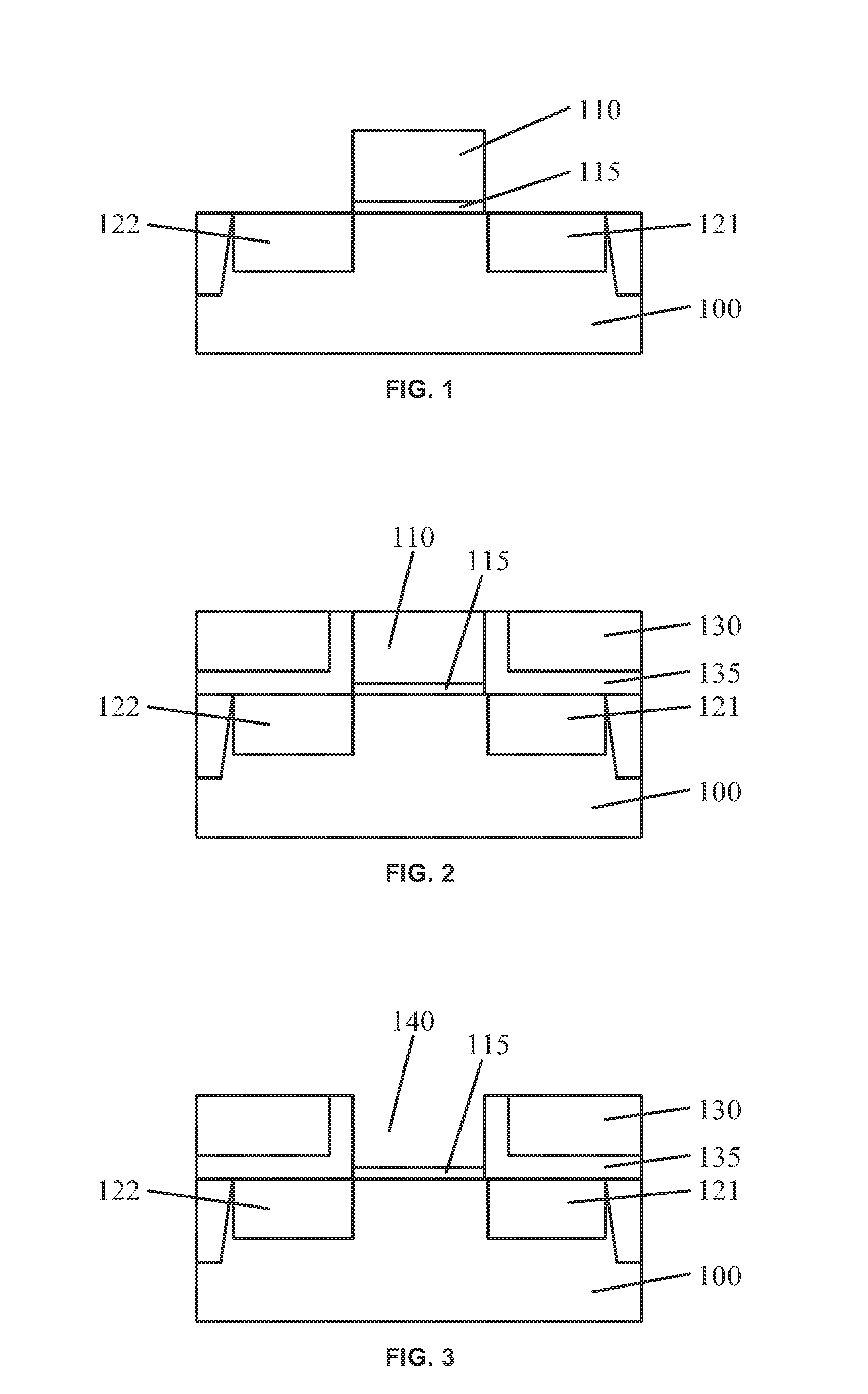
[0016]Reference will now be made in detail to exemplary embodiments of the disclosure, which are illustrated in the accompanying drawings. Wherever possible, the same reference numbers will be used throughout the drawings to refer to the same or like parts.

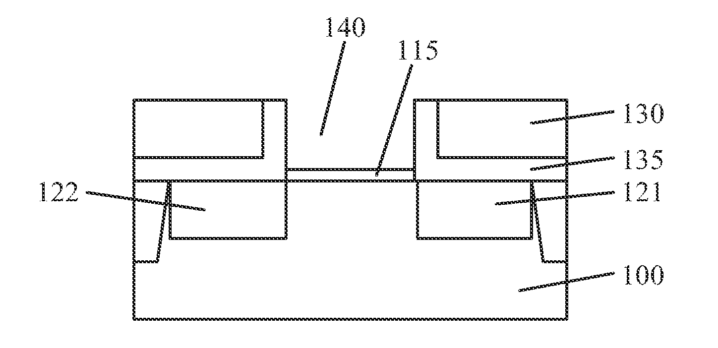
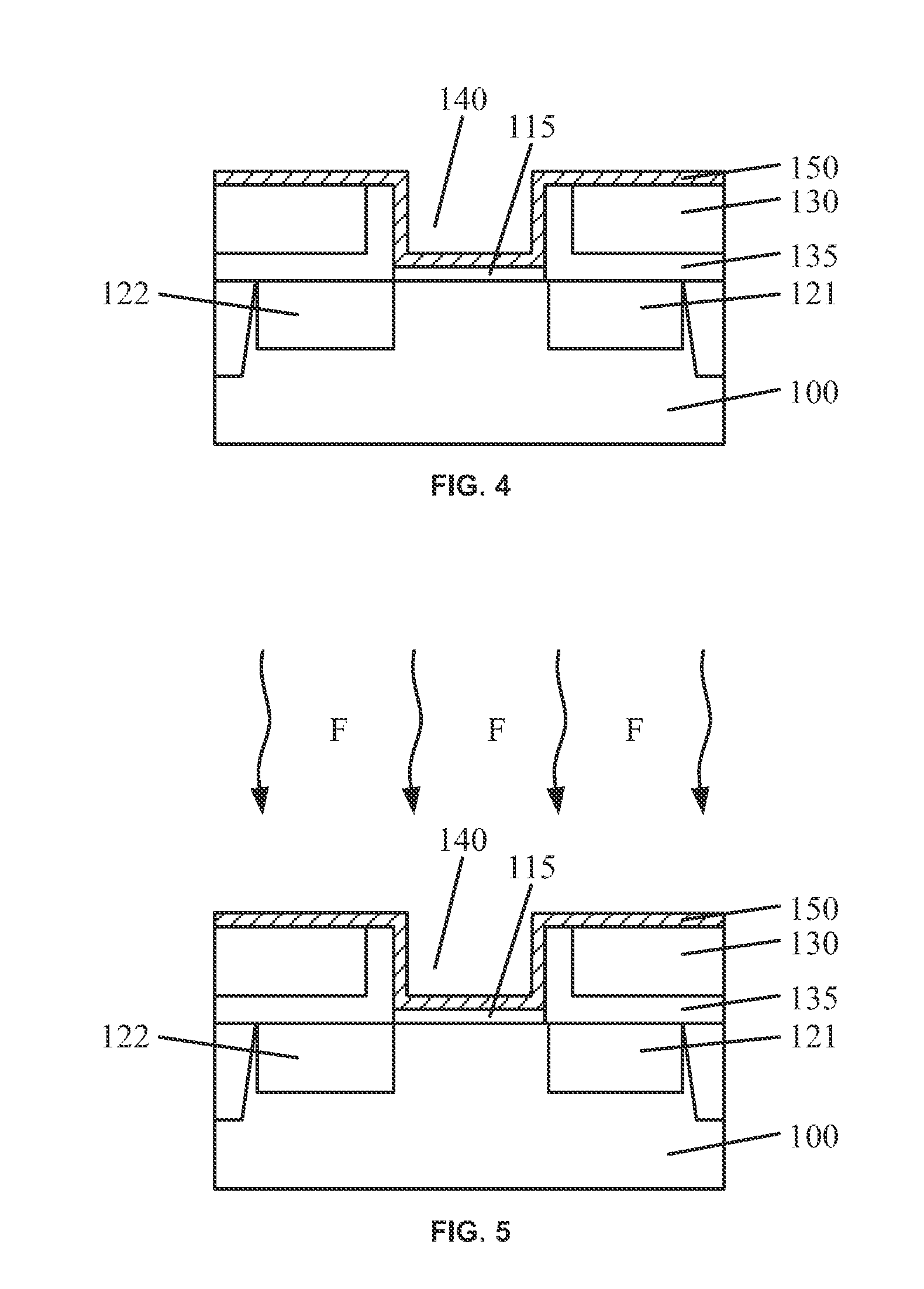
[0017]In accordance with various disclosed embodiments, to avoid interfacial defects generated at interfaces (e.g., between high-k gate dielectric layer and silicon substrate, and between high-k gate dielectric layer and metal gate electrode), high-k dielectric layers can be treated, e.g., fluorinated, during formation of a metal gate structure. For example, a trench can be formed by removing a dummy gate. A high-k gate dielectric layer can be conformally formed on the bottom and sidewall of the trench and can be fluorinated so that fluorine bonds (e.g., F—Si, F—Hf, etc.) can be formed between high-k gate dielectric layer and the semiconductor substrate.

[0018]Because the fluorine bonds have higher bond energy than hydrogen bonds g...


PUM


Abstract

Various embodiments provide transistors and their fabrication methods. An exemplary method for forming a transistor includes removing a dummy gate to form a trench over a semiconductor substrate. A high-k dielectric layer can be conformally formed on surface of the trench and then be fluorinated to form a fluorinated high-k dielectric layer. A functional layer can be formed on the fluorinated high-k dielectric layer and a metal layer can be formed on the functional layer to fill the trench with the metal layer. Due to fluorination of the high-k dielectric layer, negative bias temperature instability of the formed transistor can be reduced and oxygen vacancies can be passivated to reduce positive bias temperature instability of the transistor.

Description

CROSS-REFERENCES TO RELATED APPLICATIONS[0001]This application claims priority to Chinese Patent Application No. CN201210348153.6, filed on Sep. 18, 2012, the entire contents of which are incorporated herein by reference.FIELD OF THE DISCLOSURE[0002]The present disclosure relates to the field of semiconductor technology and, more particularly, relates to metal gate structures, MOS transistors, and CMOS transistors and their fabrication methods.BACKGROUND[0003]With the continuous development of semiconductor technologies, feature size of metal-oxide-semiconductor (MOS) transistors has been reduced. Accordingly, the thickness of gate dielectric layers in the MOS transistors has become thinner and thinner. When a gate dielectric layer is overly thinned, however, various issues may occur. These issues may include time-related voltage breakdowns, hot carrier effects, and diffusion of impurities from the gate electrode toward the substrate. This can adversely affect stability and reliabil...

Claims


Application Information

Patent Timeline
IPC IPC(8): H01L21/8238H01L29/78
CPCH01L29/78H01L21/8238H01L21/28185H01L21/28194H01L21/823842H01L29/517H01L29/66545H01L29/513
Inventor LI, AILEENNI, JINGHUA
Owner SEMICON MFG INT (SHANGHAI) CORP
Why Eureka
Try Eureka