Structure, structure-forming method, and structure-forming device
a technology of structure and structure, applied in the field of structure, structure-forming method, and structure-forming device, can solve the problems of difficult artificial development of such a structural color, and achieve the effect of improving the effect of decoration
- Summary
- Abstract
- Description
- Claims
- Application Information
AI Technical Summary
Benefits of technology
Problems solved by technology
Method used
Image
Examples
first embodiment
(1-1) First Embodiment of Structure
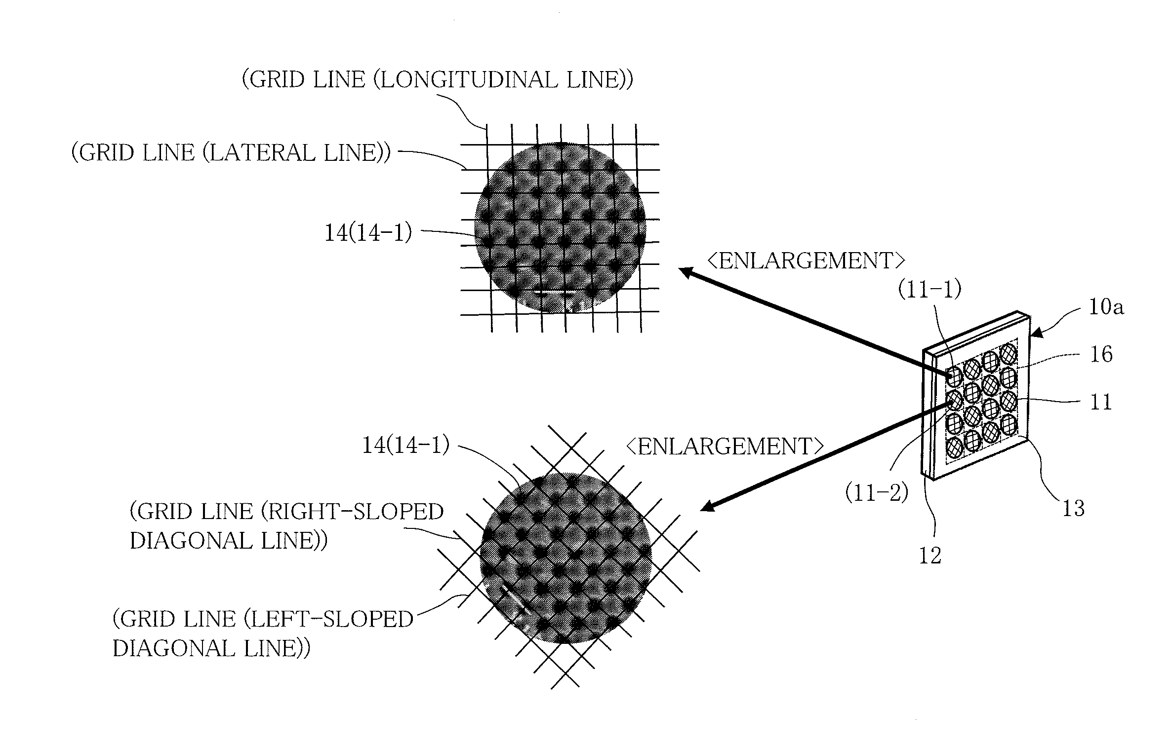
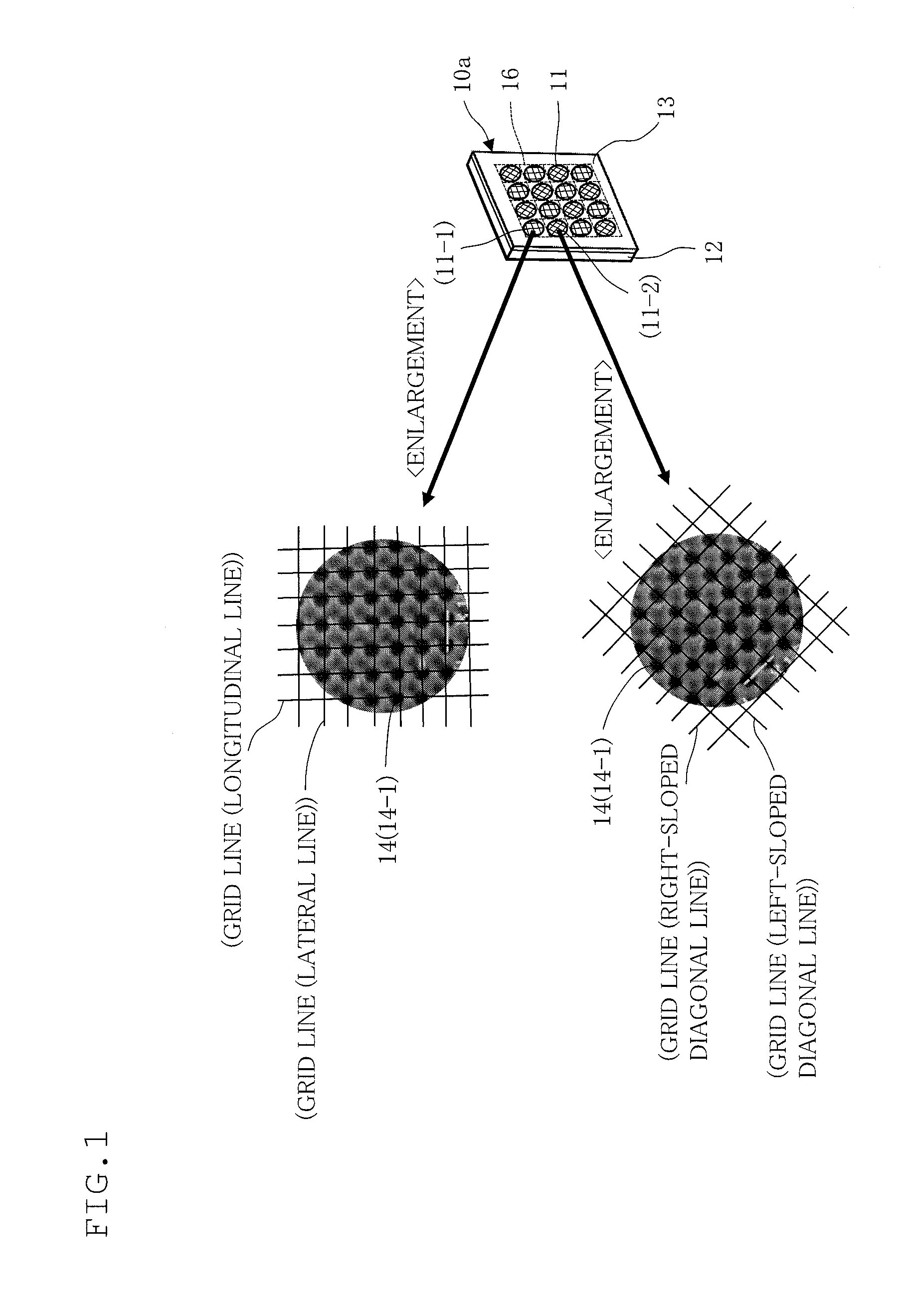
[0065]A first embodiment of a structure is described with reference to FIG. 1.
[0066]FIG. 1 represents an external perspective view showing the construction of a structure according to the present embodiment, and SEM observation images (enlarged essential part views) of fine periodic compositions formed in the structure.
[0067]As shown in FIG. 1, a structure 10a includes a plurality of regions (periodic composition forming regions) 11 having fine periodic compositions arranged in a coating 13 which is provided in the surface of a base material 12.
[0068]The fine periodic composition refers to a composition in which processed parts 14 formed by the occurrence of photodisintegration attributed to the application of pulsed laser light are arranged in the form of grid cross points.
[0069]The distance between the processed parts 14 is close to a visible light wavelength (about 400 nm to 700 nm). A large number of such processed parts 14 are periodically arr...
second embodiment
(3-2) Second Embodiment of Structure-Forming Method
[0212]In the present embodiment, the method of forming the structure 10b shown in FIG. 3 by using the structure-forming device 20 shown in FIG. 13 and the beam splitter 22b shown in FIG. 14 is described.
[0213]The laser scanner 25 has the mechanism to automatically rotate or turn or stop the first mirror 251a and the second mirror 251b at a predetermined speed.
[0214]The traveling directions of the light fluxes split in the four diffraction optical elements 221-1 to 221-4 shown in FIG. 14 are 0°, 18°, 45°, and 75°, respectively.
[0215]First, the structure 10b is located at a predetermined distance from the second lens 24 of the structure-forming device 20. This location includes the interference region where a plurality of light fluxes are crossed by the second lens 24 (see FIG. 16).
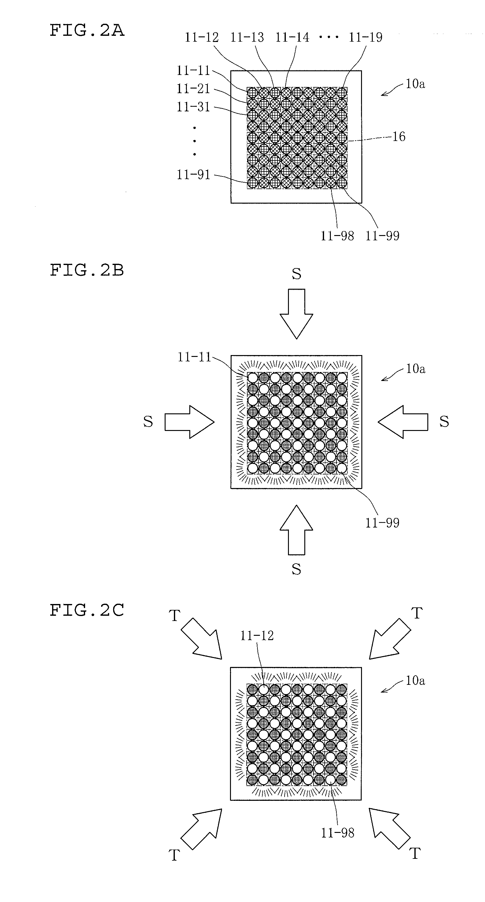
[0216]When the first mirror 251a and the second mirror 251b of the laser scanner 25 respectively reach predetermined angles (in FIG. 17A, an angle at which...
first example
[0227]Zinc oxide particles (MZ-500 manufactured by Tayca Corporation) having a mean particle diameter of 25 nm were added to an epoxy paint so that the amount of the zinc oxide particles was 40 parts by weight as compared to 100 parts by weight of a resin component of the paint. The paint was then blended.
[0228]This paint was applied to one side of an aluminum plate (having a thickness of 200 μm) to confect a sample. In this case, the thickness of a coating was about 2 μm.
[0229]Furthermore, a polyester amino paint was applied to the coating side of the confected sample, and a protective layer was confected. In this case, the thickness of the protective layer was about 6 μm.
[0230]The third harmonic of a Q-switched pulsed YAG laser (having a wavelength of 355 nm) was used as laser light to be applied. The pulse width of the pulsed YAG laser was 5 ns, and the pulse repetition frequency was 10 Hz.
[0231]The structure-forming device 20 was used to apply the laser light to the sample from ...
PUM
| Property | Measurement | Unit |
|---|---|---|
| Structure | aaaaa | aaaaa |
| Shape | aaaaa | aaaaa |
| Metallic bond | aaaaa | aaaaa |
Abstract
Description
Claims
Application Information


