Plasma treatment of film for impurity removal

a technology of impurity removal and plasma treatment, applied in the field of methods, can solve the problems of increasing processing capacity, increasing the size of circuits and devices, and reducing the extendability of techniques into less than 20 nm features, and reducing the resistance of underlying layers, so as to reduce the undesired effects of nucleation layers.

Active Publication Date: 2014-05-01
APPLIED MATERIALS INC
View PDF2 Cites 8 Cited by
  • Summary
  • Abstract
  • Description
  • Claims
  • Application Information

AI Technical Summary

Benefits of technology

[0009]Embodiments of the present invention generally provide methods of CVD deposition of metals in small features while reducing resistance of underlying layers. Specifically, the present invention generally provides methods to both control deposition of metals into trenches and vias while reducing the undesired effects of nucleation layers. In one embodiment, a method for removing impurities can include positioning a substrate with a barrier layer in a proces

Problems solved by technology

The shrinking dimensions of circuits and devices have placed additional demands on processing capabilities.
However, this technique is rapidly losing extendability into less than 20 nm features due to the increasing volume fractio

Method used


Image

  • Plasma treatment of film for impurity removal
  • Plasma treatment of film for impurity removal
  • Plasma treatment of film for impurity removal

Examples


Embodiment Construction

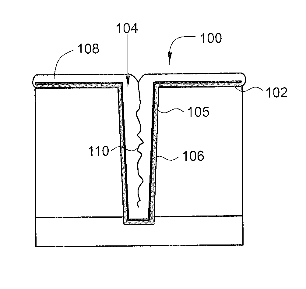
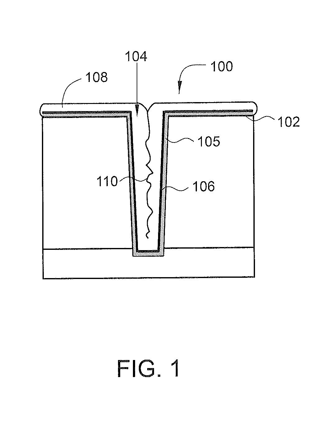
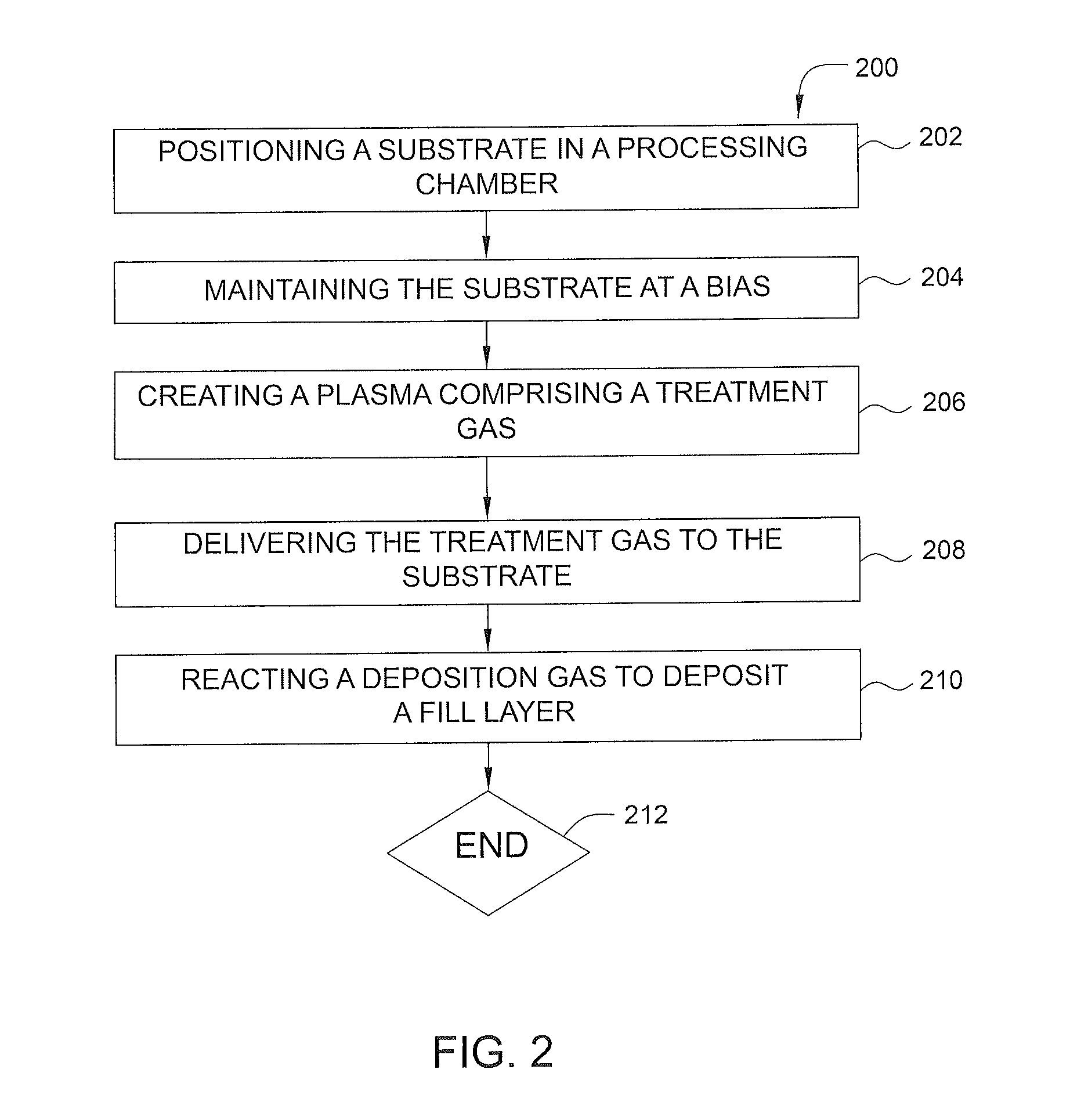
[0018]Embodiments of the present invention generally provide methods of CVD deposition of metals, such as tungsten, in small features while reducing resistance of or removing the need for underlying layers. Deposition of tungsten in features by standard techniques can lead to an increase in both the starting bulk and the overall resistance of the deposition product. Tungsten nucleation layers and in particular ALD nucleation layers from B2H6 and tungsten hexafluoride (WF6) have been successful in terms of conformality and in promoting good tungsten fill for features less than 32 nm, but are generally highly resistive compared to tungsten from WF6 and H2. Experimentally determined resistance for ALD tungsten deposited from B2H6 and WF6 is approximately 150 μΩ-cm in comparison to CVD tungsten deposition from WF6 and H2 which is less than 20 μΩ-cm. Both the ALD tungsten and the CVD tungsten are subsequently deposited on a tungsten nitride (WN) layer to increase adhesion to underlying s...


PUM

PropertyMeasurementUnit
Temperatureaaaaaaaaaa

Abstract

Methods for plasma treatment of films to remove impurities are disclosed herein. Methods for removing impurities can include positioning a substrate with a barrier layer in a processing chamber, the barrier layer comprising a barrier metal and one or more impurities, maintaining the substrate at a bias, creating a plasma comprising a treatment gas, the treatment gas comprising an inert gas, delivering the treatment gas to the substrate to reduce the ratio of one or more impurities in the barrier layer, and reacting a deposition gas comprising a metal halide and hydrogen-containing gas to deposit a bulk metal layer on the barrier layer. The methods can further include the use of diborane to create selective nucleation in features over surface regions of the substrate.

Description

CROSS-REFERENCE TO RELATED APPLICATIONS[0001]This application claims benefit of U.S. Provisional Patent Application Ser. No. 61 / 720,901 (APPM / 17580L), filed Oct. 31, 2012, which is herein incorporated by reference.BACKGROUND OF THE INVENTION[0002]1. Field of the Invention[0003]Embodiments of the invention relate generally to methods for processing a substrate during semiconductor manufacturing. Specifically, embodiments of the invention relate to methods of treating a nucleation layer prior to a CVD deposition process.[0004]2. Description of the Related Art[0005]Reliably producing nanometer-sized features is one of the key technologies for the next generation of semiconductor devices. The shrinking dimensions of circuits and devices have placed additional demands on processing capabilities. The multilevel interconnects that lie at the heart of integrated circuit technology require precise processing of high aspect ratio features, such as vias and other interconnects. Reliable format...

Claims


Application Information

Patent Timeline
IPC IPC(8): H01L21/768
CPCH01L21/28556H01L21/76843H01L21/76877H01L21/76876H01L21/76862C23C16/0227C23C16/14
Inventor WANG, BENJAMIN C.COLLINS, JOSHUAJACKSON, MICHAELGELATOS, AVGERINOS V.KHANDELWAL, AMIT
Owner APPLIED MATERIALS INC
Why Eureka
Try Eureka