Photovoltaic cell and method of manufacturing such a cell

Inactive Publication Date: 2014-05-22
STICHTING ENERGIEONDERZOEK CENT NEDERLAND
View PDF0 Cites 5 Cited by
  • Summary
  • Abstract
  • Description
  • Claims
  • Application Information

AI Technical Summary

Benefits of technology

[0027]Use of islands of fire through conductor, typic

Problems solved by technology

The corrosive effect of the molten class causes it to etch through the dielectric layer and the nearby surface of the semi-conductor body.
As a result of the use of the difference between the pastes, contact bet

Method used


Image

  • Photovoltaic cell and method of manufacturing such a cell
  • Photovoltaic cell and method of manufacturing such a cell
  • Photovoltaic cell and method of manufacturing such a cell

Examples


Example

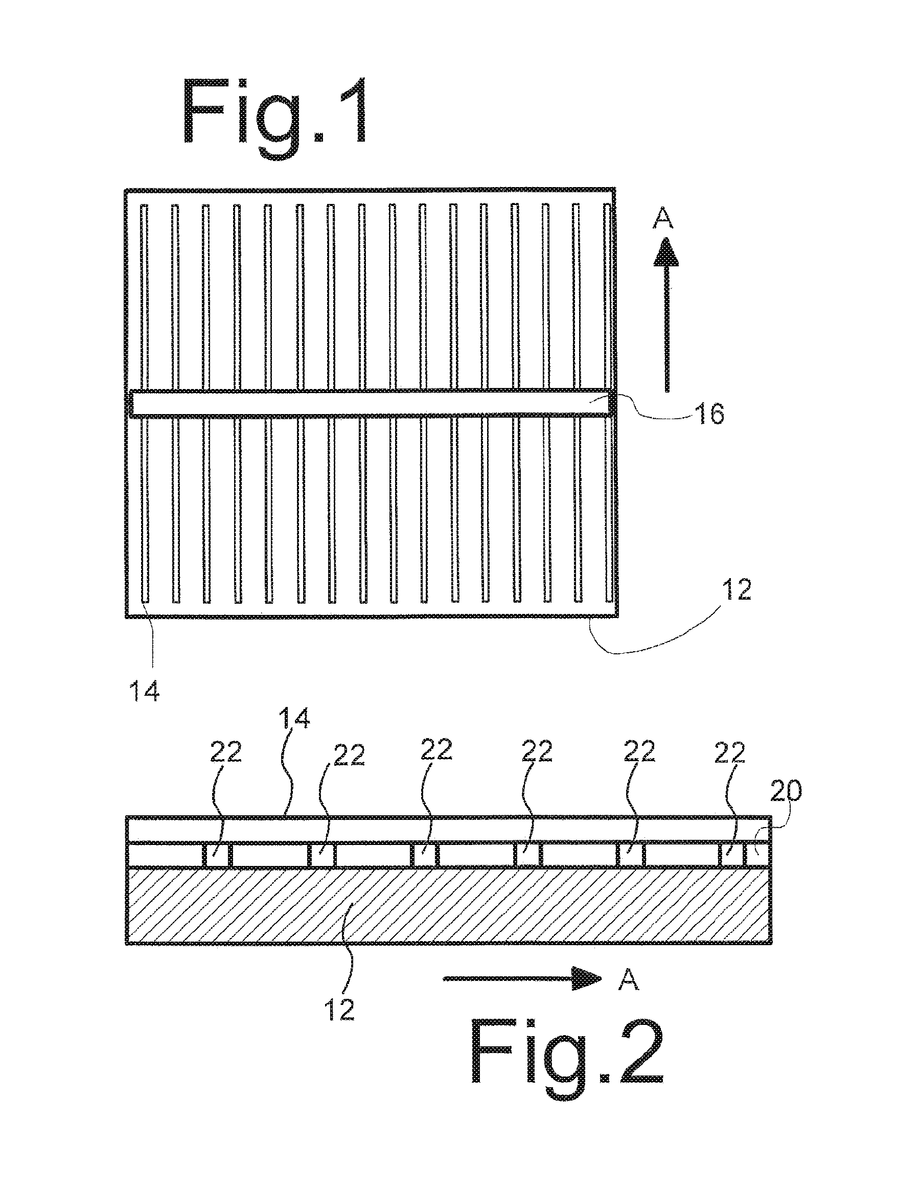
[0033]FIG. 1 shows a plane view of the top surface of a photovoltaic cell comprising an electrode structure 10 of electrically conductive material on top of a semi-conductor body 12. By way of example an electrode structure with fingers 14 and a busbar 16 is shown. Fingers 14 extend from busbar 16 along a length direction of fingers 14 indicated by arrow A.

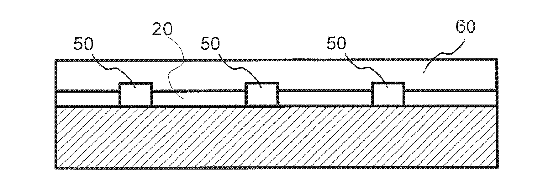
[0034]FIG. 2 shows a schematic cross section through a finger 14 along this direction. On top of semi-conductor body 12 a dielectric layer 20 is provided. Between finger 14 and semi-conductor body 12 a plurality of contacts 22 is provided through dielectric layer 20. Contacts 22 are made of fire through material, i.e. typically of sintered conductor grains.

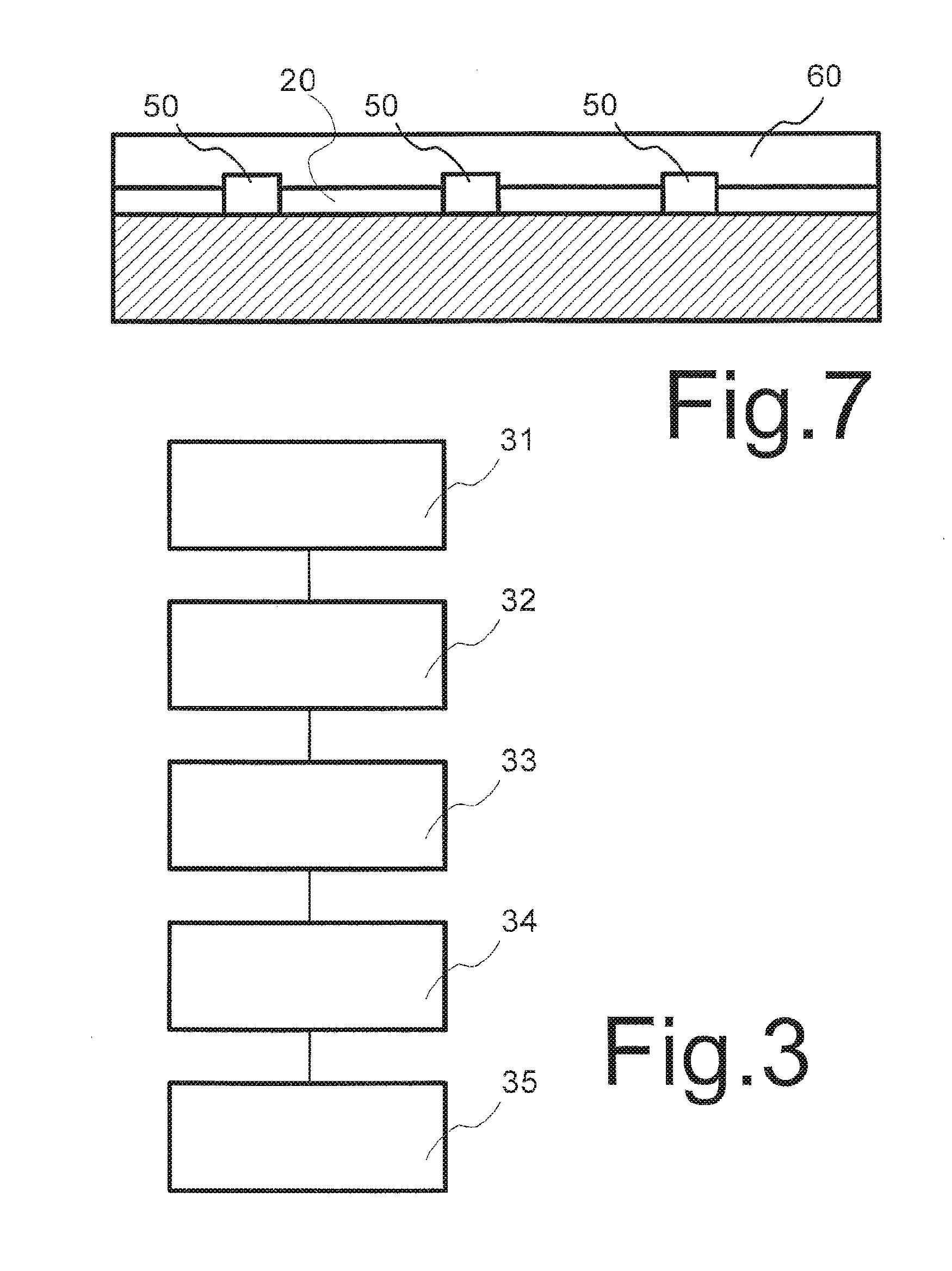
[0035]FIG. 3 shows a flow-chart of a process of manufacturing a photovoltaic cell. After a number of conventional preparatory steps, symbolized by first step 31, this process provides for an intermediate product comprising a semi-conductor body with a dielectric layer on top, bu...


PUM


Abstract

A fire through conductor paste is applied as a plurality of mutually separate islands on a dielectric layer on a semi-conductor body of a photo-voltaic cell. A connecting structure of a further conductor paste is applied connecting the islands, at least on the dielectric layer between locations of the islands, so that the islands are connected by the connecting structure. Different compositions are used for the fire through conductor paste and the further conductor paste, which behave differently during firing. The fire through conductor paste and the further conductor paste are fired under process conditions wherein the fire through conductor paste fires through the dielectric layer and the further conductor paste does not fire through the dielectric layer. In this way the fire through metal paste establishes electric contact through the dielectric layer between the semi-conductor body and a structure formed from the further conductor paste.

Description

FIELD OF THE INVENTION[0001]The invention relates to a photovoltaic cell and a method of manufacturing a photovoltaic cell.BACKGROUND[0002]A photovoltaic cell such as a solar cell, comprises a semi-conductor body with electrodes on its surface, in electric contact with the semi-conductor body.[0003]U.S. Pat. No. 5,279,682 discloses a solar cell with a bus bar removed from intimate contact with the semi-conductor body. The cell has fingers in low resistance electrical contact with the semiconductor substrate and a bus bar of conductive material disposed at right angles to the fingers and in low resistance electrical contact with the front surfaces of each of the fingers. The fingers are made of a paste or viscous ink designed to make intimate contact with the underlying semiconductor substrate. The bus bar is formed of a selected paste or viscous ink or an epoxy composition containing particles of a conductive metal applied to the front surface of the anti-reflective coating at right...

Claims


Application Information

Patent Timeline
IPC IPC(8): H01L31/0224
CPCH01L31/022425Y02E10/50
Inventor GEERLIGS, LAMBERT JOHAN
Owner STICHTING ENERGIEONDERZOEK CENT NEDERLAND
Why Eureka
Try Eureka