Plasma etching method

a technology of etching method and plasma, which is applied in the direction of electrical equipment, optical objects, domestic applications, etc., can solve the problems of shrinkage of device feature dimensions, difficulty in maintaining the height necessary to etch the antireflective coating and the rest, so as to reduce the variation of feature dimension

Inactive Publication Date: 2014-06-05
HITACHI HIGH-TECH CORP
View PDF8 Cites 2 Cited by
  • Summary
  • Abstract
  • Description
  • Claims
  • Application Information

AI Technical Summary

Benefits of technology

The present invention provides a plasma etching method that uses an EUV-exposed resist to reduce feature dimension variations. This means that this method can make sure that the dimensions of the features are uniform and accurate. As a result, this method can help improve the performance and reliability of the plasma etching process.

Problems solved by technology

H11 (1999)-135476, the resist shrinks drastically because the strong reaction of O2 gas with the resist causes side etching of the resist, and therefore it makes it difficult for the resist to maintain the height necessary to etch the antireflective coating and the rest.
This results in shrinkage of device feature dimensions.
In addition, the EUV-exposed resist would make this problem more pronounced because the resist is relatively thin.

Method used


Image

  • Plasma etching method
  • Plasma etching method
  • Plasma etching method

Examples


Embodiment Construction

[0020]With reference to the drawings, an embodiment of the present invention will be described below.

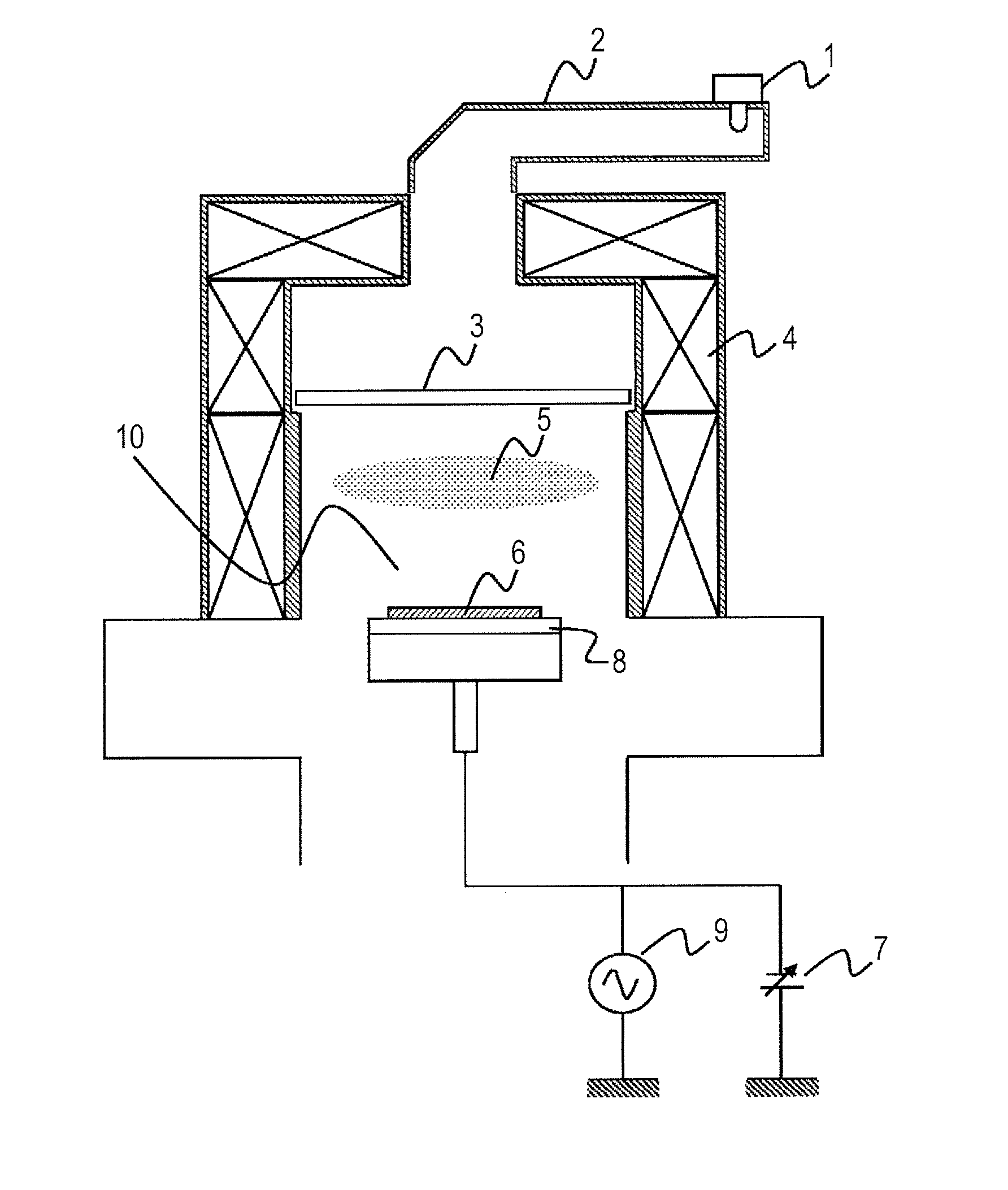
[0021]The description starts with a plasma etching system used to implement the present invention. FIG. 1 is a schematic cross-sectional view of an electron cyclotron resonance (ECR) microwave plasma etching system utilizing microwaves and magnetic fields to generate plasma.

[0022]Microwaves generated in a magnetron 1 pass through a quartz plate 3 via a waveguide 2 to be transferred to a vacuum chamber 10. The vacuum chamber 10 is surrounded by solenoidal coils 4. A magnetic field generated by the solenoidal coils 4 and the microwaves transferred to the vacuum chamber 10 produce electron cyclotron resonance (hereinafter referred to as ECR). The ECR efficiently converts process gas into high density plasma.

[0023]A wafer 6, which is a specimen, is attracted onto a wafer stage 8 by electrostatic attraction force generated by applying DC voltage from an power source for electrostatic chuc...


PUM


Abstract

The present invention provides a plasma etching method with an EUV-exposed resist capable of preventing variations of device feature dimensions. The plasma etching method of the present invention is to plasma-etch a target material with a multilayer resist that serves as a mask and composed of an EUV-exposed resist, an antireflective coating, an inorganic film and an organic film. The plasma etching method includes a first step of depositing a deposition film on a surface of the EUV-exposed resist before the antireflective coating is etched, a second step of etching the deposition film deposited on the antireflective coating and the antireflective coating with a gas mixture of Cl2 gas, HBr gas and N2 gas after the first step, a third step of etching the inorganic film after the second step, and a fourth step of etching the organic film after the third step.

Description

CLAIM OF PRIORITY[0001]The present application claims priority from Japanese patent application JP 2012-261847 filed on Nov. 30, 2012, the content of which is hereby incorporated by reference into this application.BACKGROUND OF THE INVENTION[0002]1. Field of the Invention[0003]The present invention relates to plasma etching methods for semiconductor devices. More particularly, the present invention relates to a plasma etching method including formation of a multilayer resist mask.[0004]2. Description of the Related Art[0005]In current semiconductor device fabrication technologies for the 45-nm node and beyond, an immersion lithography system, which includes an ArF laser source to apply ArF laser light to a wafer with purified water introduced between the wafer and a projection lens, is used for mask patterning. To respond to demands for still higher resolution patterning to fabricate 22-nm node semiconductor devices and beyond, next-generation extreme ultraviolet (EUV) lithography t...

Claims


Application Information

Patent Timeline
IPC IPC(8): B29D11/00
CPCB29D11/0074H01L21/0276H01L21/0332H01L21/31116H01L21/31138H01L21/3065
Inventor UNE, SATOSHIISHIMURA, HIROAKIMATSUDA, KOUHEI
Owner HITACHI HIGH-TECH CORP
Why Eureka
Try Eureka