Spin transfer torque magnetic memory device using magnetic resonance precession and the spin filtering effect

Inactive Publication Date: 2014-06-12
SAMSUNG ELECTRONICS CO LTD
7 Cites 47 Cited by

AI-Extracted Technical Summary

Problems solved by technology

If an external magnetic field is used in order to control the magnetization of a free layer, a half-selected cell problem occurs with the reduction of a size of a device to limit high integration of the device.
This is a limitation of super-paramagnetism and causes a problem that a written magnetic data is undesirably erased.
In addition, because the amount of a current provided in a complementary metal-oxide-semiconductor (CMOS) transistor device is limited, a low critical current density for the magnetization reversal of the free magnetic layer is required.
However, the ...

Method used

[0053]According to the present invention, in a magnetic memory device, thermal stability is maintained and a critical current density is reduced to reduce a device size. Thus, high integration is realized and usage power consumption is reduced in writing. Additionally, characteristics of the device are not deteriorated by a stray field generated from a fixed magnetic layer. To achieve these, the present invention provides a new structural magnetic memory device that induces an alternating current (AC) magnetic field in itself and controls this.
[0055]In other words, the second free magnetic layer 205 having horizontal anisotropy is additionally inserted in the first free magnetic layer 203 having perpendicular anisotropy, so that the magnetization of the second free magnetic layer is rotated by a spin-transfer-torque effect when a current is applied and so that a direct current (DC) is applied to rotate the magnetization in a plane of the free layer with a high frequency. As a result, an alternating current (AC) magnetic field having the high frequency is autonomously generated to be possible to effectively reduce the critical current density of the device.
[0057]In other words, the second free magnetic layer 305 having horizontal anisotropy is additionally inserted in the first free magnetic layer 303 having perpendicular anisotropy, so that the second free magnetic layer performs a precessional motion through the spin-transfer-torque effect to generate a high frequency alternating current (AC) magnetic field. The high frequency alternating current (AC) magnetic field is possible to reduce the critical current density of the device.
[0059]Also, the magnetization direction of the first fixed magnetic layer and the magnetization direction of the second fixed magnetic layer may be controlled to reduce the stray field applied to the first free magnetic layer as compared with a conventional device. Thus, the thermal stability of magnetization data written in the device may be improved.
[0064]Thus, the second free magnetic layer 205 rotated at the high ...

Benefits of technology

[0037]The magnetic memory device having a new structure according to the present invention further includes the free magnetic layer constituting a horizontal direction variable magnetization layer having a fixed saturation magnetization value, whereby a switching current is markedly reduced as compared with conventional magnetic layers such ...

Abstract

The present invention relates to a magnetic memory device which additionally comprises a free magnetic layer constituting a horizontal direction variable magnetization layer having a fixed saturation magnetization value, whereby a switching current is markedly reduced as compared with conventional magnetic layers such that a high degree of integration of the device can be achieved and it is possible to lower a critical current density necessary for magnetization reversal thereby reducing the power consumption of the device. Also, a stray field effect occurring from a fixed magnetic layer is reduced such that a written magnetization data is thermally stable.

Application Domain

Galvano-magnetic device detailsDigital storage +1

Technology Topic

Spin filteringCritical current +11

Image

  • Spin transfer torque magnetic memory device using magnetic resonance precession and the spin filtering effect
  • Spin transfer torque magnetic memory device using magnetic resonance precession and the spin filtering effect
  • Spin transfer torque magnetic memory device using magnetic resonance precession and the spin filtering effect

Examples

  • Experimental program(5)

Example

Experimental Example 1
Magnetization Behavior of First Free Magnetic Layer and Second Free Magnetic Layer According to a Time Caused by Applying a Current to the Device According to the Present Invention
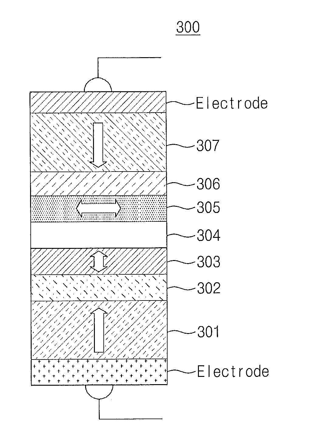
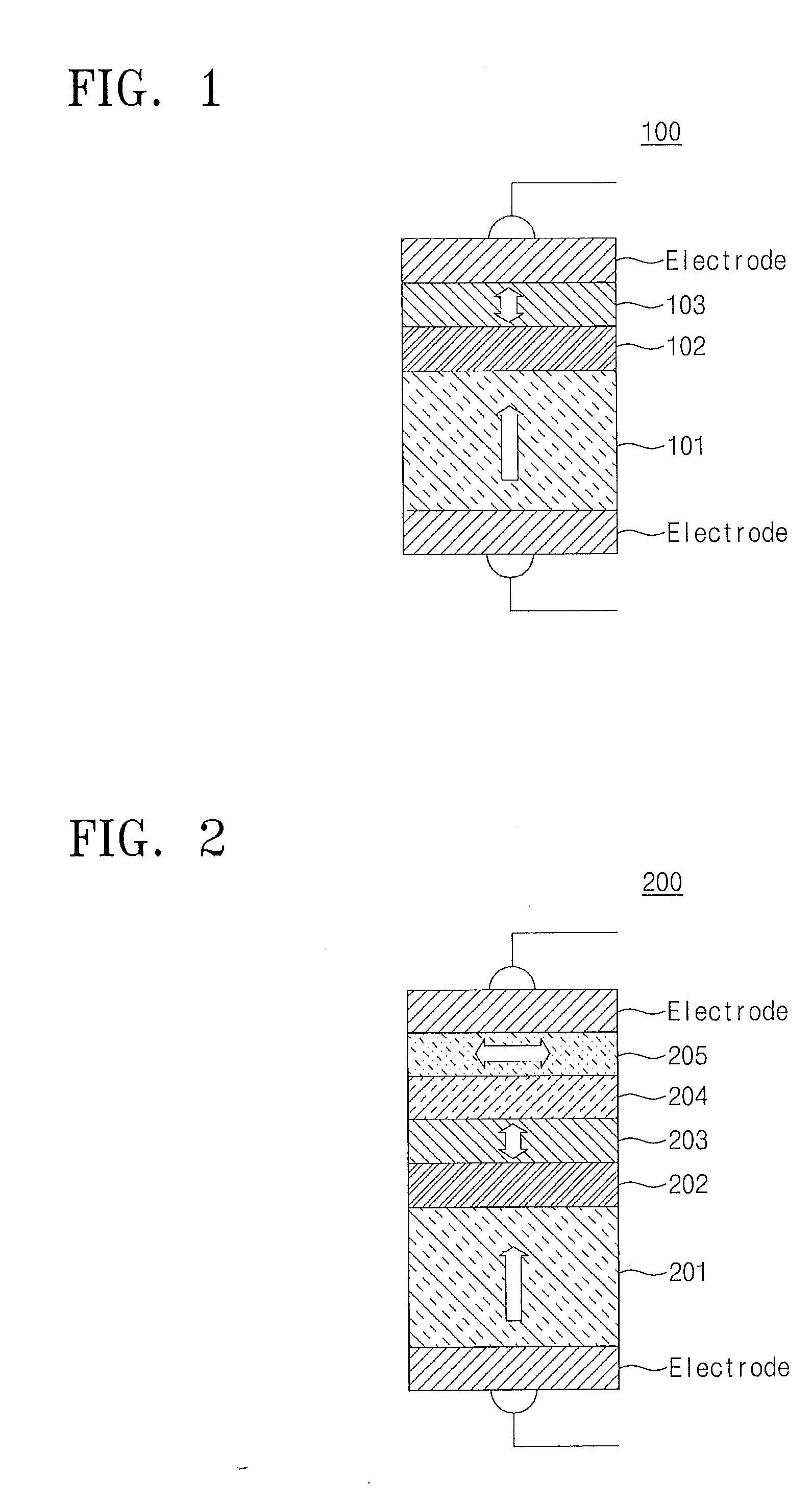
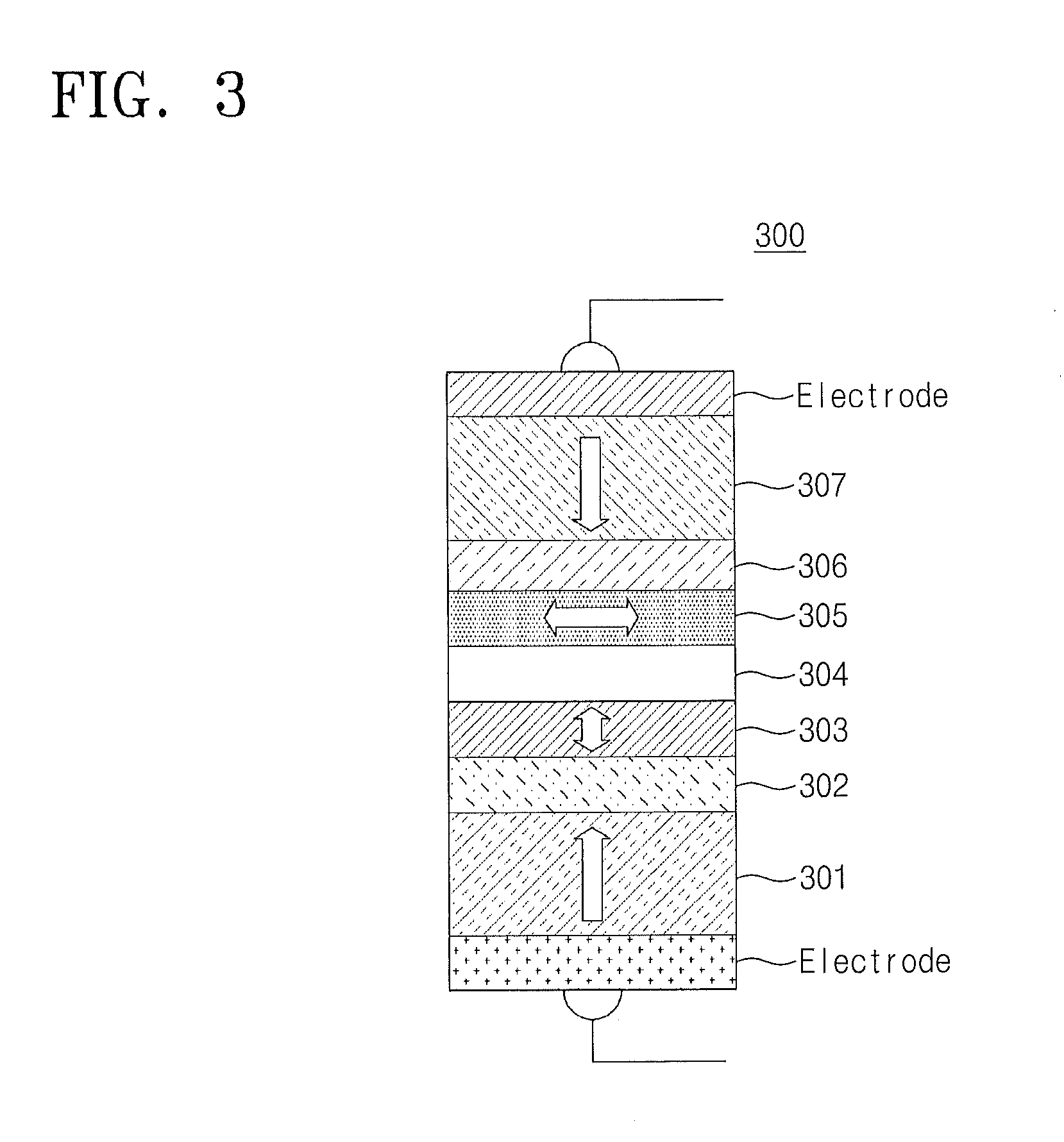
[0077](1) There is illustrated magnetization behavior of the first free magnetic layer having the perpendicular anisotropy and the second free magnetic layer having the horizontal anisotropy when the current is applied to the magnetic memory device according to an embodiment of the present invention as shown in the following FIG. 2.
[0078](2) Structure and physical property values of the device are as follows:
[0079]sectional area of an entire structure=314 nm2,
[0080]fixed magnetic layer 201/first non-magnetic layer 202/first free magnetic layer 203: “thickness (t)=3 nm, perpendicular anisotropy constant (K⊥)=6×10⁶ erg/cm3, saturation magnetization value (MS1)=1000 emu/cm3, Gilbert damping constant (α)=0.01, and spin polarization efficiency constant (η1)=1.0”,
[0081]second non-magnetic layer 204: thickness t=1 nm, and
[0082]second free magnetic layer 205: “thickness (t)=1 nm, perpendicular anisotropy constant (K⊥)=0 erg/cm3, saturation magnetization value (MS2)=700 emu/cm3, Gilbert damping constant (α)=0.01, and spin polarization efficiency constant (η2)=1.0”.
[0083](3) The following FIG. 4A is a graph showing an applied current according to a time. A current pulse having a rise time of 40 ps and a width of 5 ns was applied in order to observe switching behavior of the magnetization.
[0084]The following FIG. 4B is a graph showing the magnetization behavior of the first free magnetic layer 203 according to a time.
[0085]Referring to the following FIG. 4B, an x-component being a horizontal direction to the plane of the layer oscillates according to the time, and a z-component is changed from +1000 emu/cm3 to −1000 emu/cm3 at a time (t) of about ins. This means that a magnetization component is switched by the applied current.
[0086]The following FIG. 4C is a graph showing magnetization behavior of the second free magnetic layer 205 according to a time.
[0087]Referring to the following FIG. 4C, a component in a plane (i.e., an x-axis component) of the magnetization of the second free magnetic layer 205 is very greater than a perpendicular component (i.e., an z-axis component) of the magnetization of the second free magnetic layer 205, and the second free magnetic layer 205 shows behavior oscillating according to a time with the same period as the magnetization of the first free magnetic layer 203. The oscillation (i.e., precessional motion) according to the time of the second free magnetic layer 205 occurs by perpendicular directional spin torque spin-polarized by the first free magnetic layer 203 magnetized in a perpendicular direction when the current is applied to the entire structure.
[0088]The following FIG. 4D is a graph showing an alternating current (AC) magnetic field generated in the first free magnetic layer 203 by the precessional motion of the second free magnetic layer 205 according to the time. The alternating current (AC) magnetic field is a magnetic field that is generated by the magnetization of the second free magnetic layer 205 in a position of the first free magnetic layer 203. This occurs because of the precessional motion of the magnetization of the second free magnetic layer 205 according to the time.
[0089]Referring to the following FIG. 4D, the alternating current (AC) magnetic field having an x-component and a magnitude of about 200 Oe is autonomously generated in the magnetic memory device structure according to the present invention. Thus, the device structure according to the present invention does not require an external additional element generating an alternating current (AC) magnetic field in order to reduce a current density for reversing the magnetization of the first free magnetic layer 203, unlike a conventional device structure.
[0090]In other words, since the component in the plane of the second free magnetic layer 205 does the precessional motion, the x-component of the alternating current (AC) magnetic field induced in the first free magnetic layer is very greater than a z-component of the alternating current (AC) magnetic field. As a result, the induced magnetic field reduces anisotropy energy of a magnetization easy axis (z-axis) of the first free magnetic layer 203 such that the magnetization switching of the first free magnetic layer 203 is easy.

Example

Experimental Example 2
Measurement of Switching Probabilities with Respect to Currents Applied to a Device According to the Present Invention and a Device According to a Conventional Structure
[0091](1) There are illustrated switching currents with respect to the conventional structure of FIG. 1 and the new structure according to the present invention of FIG. 2.
[0092](2) Structure and physical property values of the devices are as follows.
[0093]A sectional area of an entire structure of each of the two structures is 314 nm2.
[0094]The conventional structure of FIG. 1 has fixed magnetic layer 101/non-magnetic layer 102/free magnetic layer 103: “thickness (t)=3 nm, perpendicular anisotropy constant (K⊥)=6×10⁶ erg/cm3, saturation magnetization value (MS1)=1000 emu/cm3, Gilbert damping constant (α)=0.01, and spin polarization efficiency constant (η1)=1.0”.
[0095]The physical property values of the new structure according to the present invention are as follows:
[0096]fixed magnetic layer 201/first non-magnetic layer 202/first free magnetic layer 203: “thickness (t)=3 nm, perpendicular anisotropy constant (K⊥)=6×10⁶ erg/cm3, saturation magnetization value (MS1)=1000 emu/cm3, Gilbert damping constant (α)=0.01, and spin polarization efficiency constant (η1)=1.0”,
[0097]second non-magnetic layer 204: thickness t=1 nm, and second free magnetic layer 205: “thickness (t)=1 nm, perpendicular anisotropy constant (K⊥)=0 erg/cm3, saturation magnetization value (MS2)=700 emu/cm3, Gilbert damping constant (α)=0.01, and spin polarization efficiency constant (η2)=1.0”.
[0098]The fixed magnetic layer, the non-magnetic layer and the free magnetic layer of the conventional structure have the same structures and the same physical property values as the fixed magnetic layer, the first non-magnetic layer and the first free magnetic layer of the new structure according to the present invention.
[0099](3) In the present experimental example, a temperature of the device is 300K, and the experiment was repeated 100 times with respect to each applied current, thereby measuring probability of magnetization switching.
[0100]The following FIG. 5A is a graph showing switching probabilities PSW according to applied currents of the new structure (FIG. 2) according to the present invention and the conventional structure (FIG. 1).
[0101]Referring to the following FIG. 5A, a switching current is defined as a current having a switching probability PSW of 0.5. The switching current of the new structure was 7.9 μA and the switching current of the conventional structure was 17.6 μA. In other words, this means that the switching current is reduced by about 55%.
[0102]The following FIG. 5B is a graph showing values obtained by differentiating the switching probabilities shown in FIG. 5A with a current.
[0103]Referring to the following FIG. 5B, a Q-factor is a value obtained by dividing an x-axis value of a peak by a width of a distribution functions at a position having a y-axis value of 0.5 (i.e., full width half maximum (FWHM)) in a general probability distribution. In the present experimental example, the Q-factor is defined as Ic/ΔI. The Q-factor of the new structure of FIG. 2 according to the present invention is 13.5, and the Q-factor of the conventional structure of FIG. 1 is 3.6.
[0104]In other words, the high Q-factor of the magnetic memory device structure according to the present invention means that the switching probability distribution is small. This means that dispersion of the current applied for changing a magnetization state is small. Thus, the magnetic memory device structure according to the present invention is excellent in commercialization.

Example

Experimental Example 3
Measurement of a Switching Current According to a Saturation Magnetization Value of the Second Free Magnetic Layer 205 in the Device According to the Present Invention
[0105](1) There is illustrated variation of the switching current according to the saturation magnetization value (MS2) of the second free magnetic layer 205 in the new structure according to the present invention.
[0106](2) Structure and physical property values of the device are as follows:
[0107]sectional area of an entire structure=314 nm2,
[0108]fixed magnetic layer 201/first non-magnetic layer 202/first free magnetic layer 203: “thickness (t)=3 nm, perpendicular anisotropy constant (K⊥)=6×10⁶ erg/cm3, saturation magnetization value (MS1)=1000 emu/cm3, Gilbert damping constant (α)=0.01, and spin polarization efficiency constant (η1)=1.0”,
[0109]second non-magnetic layer 204: thickness t=1 nm, and
[0110]second free magnetic layer 205: “thickness (t)=1 nm, perpendicular anisotropy constant (K⊥)=0 erg/cm3, saturation magnetization value (MS2)=0-2000 emu/cm3, Gilbert damping constant (α)=0.01, and spin polarization efficiency constant (η2)=0-1.0”.
[0111]In the present experimental example, a temperature of the device is 300K, and switching probability was measured after the experiment was repeated 100 times with respect to each applied current like the experimental example 2.
[0112]The following FIG. 6 is a graph showing a switching current with respect to the saturation magnetization value and the spin polarization efficiency of the second free magnetic layer 205.
[0113]Referring to the following FIG. 6, the switching current is varied according to the saturation magnetization value (MS2) of the second free magnetic layer 205 having the horizontal anisotropy. Here, a case having the saturation magnetization value (MS2) of 0 emu/cm3 corresponds to a structure not including the second free magnetic layer, i.e., the conventional magnetic memory device structure of FIG. 1. According to the present invention, if the saturation magnetization value (MS2) is 300 emu/cm3 or more, the switching current is reduced as compared with the conventional structure regardless of the spin polarization efficiency of the second free magnetic layer 205. In particular, the reduction effect of the switching current is greatest when the saturation magnetization value (MS2) is in a range of 300 emu/cm3 to 500 emu/cm3.
[0114]As described above, the induced alternating current (AC) magnetic field of the second free magnetic layer 205 is required in order to reduce the switching current of the first free magnetic layer 203. As described in the present experimental example, the reduction effect of the switching current density is produced when the saturation magnetization value (MS2) of the second free magnetic layer 205 is 300 emu/cm3 or more.
[0115]The new magnetic memory device structure according to the present invention includes the second free magnetic layer 205 having the saturation magnetization value equal to or greater than a certain value and the horizontal anisotropy such that the switching current is effectively reduced as compared with the conventional structure.

PUM

no PUM

Description & Claims & Application Information

We can also present the details of the Description, Claims and Application information to help users get a comprehensive understanding of the technical details of the patent, such as background art, summary of invention, brief description of drawings, description of embodiments, and other original content. On the other hand, users can also determine the specific scope of protection of the technology through the list of claims; as well as understand the changes in the life cycle of the technology with the presentation of the patent timeline. Login to view more.

Similar technology patents

Automatic disc loading device suitable for small-volume bottled discs

ActiveCN106184873AReasonable structural designHigh degree of integrationPackaging bottlesVolumetric flaskEngineering
Owner:连云港千樱医疗设备有限公司

Classification and recommendation of technical efficacy words

  • High degree of integration
  • Low density

Nitride semiconductor laser device

ActiveUS20090141765A1Improve life characteristicsLow densityOptical wave guidanceLaser detailsElectron blocking layerLaser
Owner:ROHM CO LTD
Why Eureka
Try Eureka