
Integrated Photonic Devices with Reduced Sensitivity to External Influences

a technology external influences, which is applied in the field of integrated photonic devices with reduced sensitivity to external influences, can solve the problems of ionizing radiation, temperature dependence of device characteristics, geometrical variations,

Active Publication Date: 2014-06-12
INTERUNIVERSITAIR MICRO ELECTRONICS CENT (IMEC VZW) +1
View PDF5 Cites 17 Cited by
  • Summary
  • Abstract
  • Description
  • Claims
  • Application Information

AI Technical Summary

Benefits of technology

The invention provides better methods and devices for creating photons that are less sensitive to external influences.

Problems solved by technology

The sensitivity of on-chip integrated photonic devices to external effects acting on the chip or on the local environment of the photonic device is a major issue, in particular for integrated photonic devices with an intentional wavelength-dependent transmission or filter characteristic.
The dependence of device characteristics on temperature, geometrical variations (e.g. related to manufacturing tolerances) and / or ionizing radiation, is undesirable for such integrated photonic devices.
For example, the problem of temperature sensitivity is in particular pronounced for photonic devices made in a material having a high dependence of refractive index on temperature (i.e. a high thermo-optic coefficient).
Therefore, temperature dependence is one of the fundamental limitations of silicon photonic devices, because of the high thermo-optic coefficient of silicon (1.86×10⁻⁴ K−1).
It is a challenge to reduce the temperature sensitivity of such photonic devices, in particular photonic devices with a wavelength-dependent transmission or filter characteristic, especially in combination with a low propagation loss and small footprint.
However, the use of such an overlay may lead to aging problems and thermal hysteresis.
Moreover, a polymer overlay cannot withstand high-temperature treatments typically used in back-end metallization in CMOS processes.
Therefore the use of such a polymer overlay is not CMOS compatible.
However, this requires active temperature monitoring which is space consuming and leads to high power consumption.

Method used


Image

  • Integrated Photonic Devices with Reduced Sensitivity to External Influences
  • Integrated Photonic Devices with Reduced Sensitivity to External Influences
  • Integrated Photonic Devices with Reduced Sensitivity to External Influences

Examples


Embodiment Construction

[0053]In the following detailed description, numerous specific details are set forth in order to provide a thorough understanding of the invention and how it may be practiced in particular embodiments. However, it will be understood that the present invention may be practiced without these specific details. In other instances, well-known methods, procedures and techniques have not been described in detail, so as not to obscure the present invention. While the present invention will be described with respect to particular embodiments and with reference to certain drawings, the invention is not limited hereto. The drawings included and described herein are schematic and are not limiting the scope of the invention. It is also noted that in the drawings, the size of some elements may be exaggerated and, therefore, not drawn to scale for illustrative purposes.

[0054]Furthermore, the terms first, second, third and the like in the description, are used for distinguishing between similar ele...


PUM

PropertyMeasurementUnit
lengthaaaaaaaaaa
widthaaaaaaaaaa
widthaaaaaaaaaa

Abstract

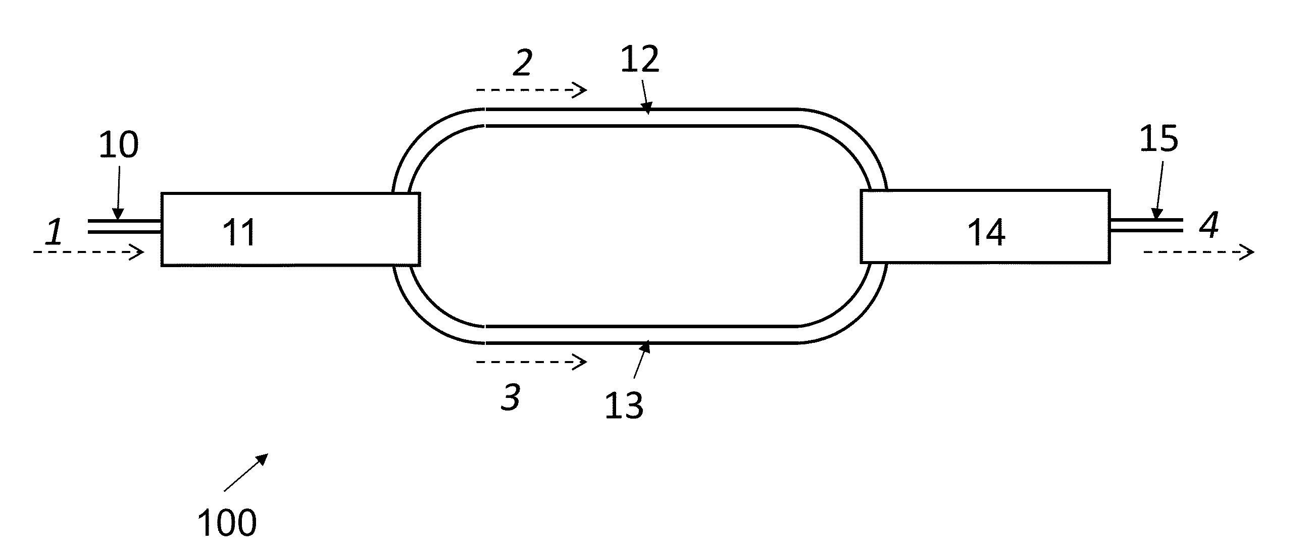
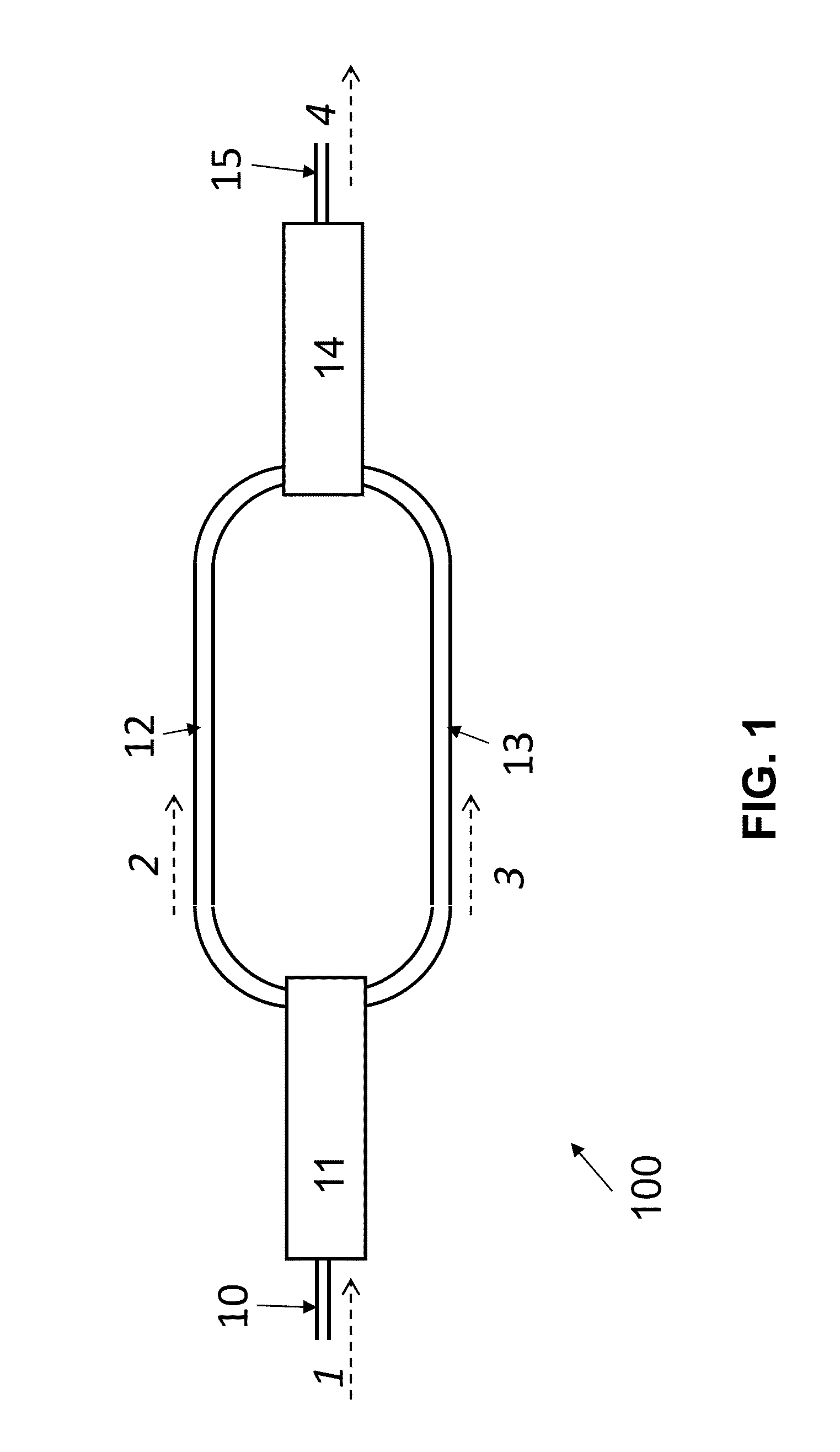
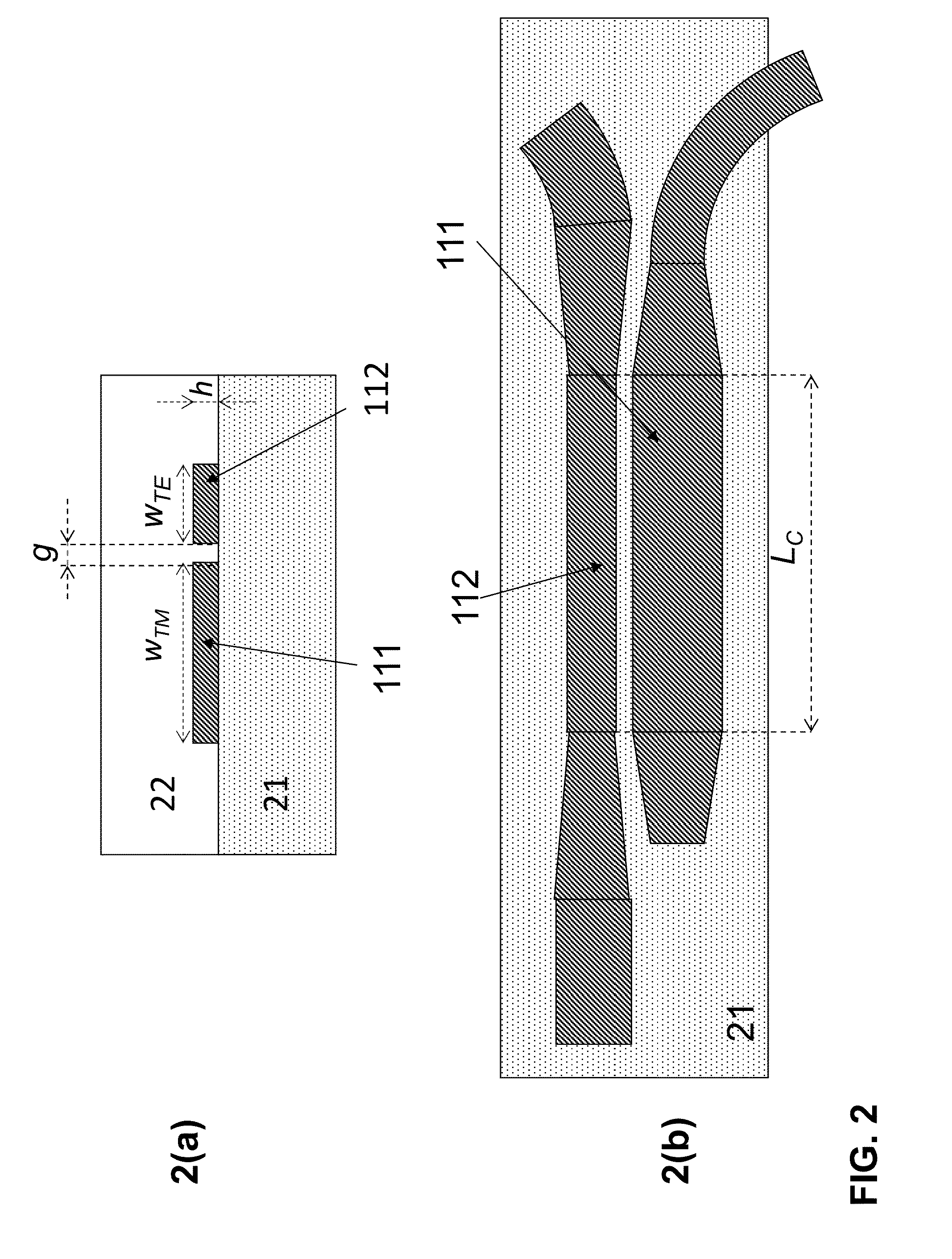
One aspect of the invention relates to a photonic device having a wavelength-dependent transmission or filter characteristic, comprising: a Splitter Polarization Rotator receiving polarized light and providing a first resp. second wave; a first resp. second waveguide arm connected to the SPR for propagating a first resp. second polarization mode (TM, TE) of the first resp. second wave, the second polarization mode being different from the first polarization mode; and a Polarization Rotator and Combiner for combining the propagated first resp. second waves; wherein the dimensions of the first and second arm are selected to cancel the influence of an external effect on the wavelength-dependent characteristic. Another aspect of the invention relates to a method for reducing the sensitivity of said integrated photonic device, comprising splitting a polarized light beam, propagating light waves of different polarity through two waveguide arms of specific dimensions, and recombining them.

Description

CROSS-REFERENCE TO RELATED APPLICATIONS[0001]This application claims the benefit of priority of U.S. Provisional Patent Application Ser. No. 61 / 734,042, filed Dec. 6, 2012, which is hereby incorporated herein by reference in its entirety.FIELD OF THE INVENTION[0002]The present invention relates in certain aspects to methods for reducing the sensitivity of on-chip integrated photonic devices having a wavelength-dependent transmission or filter characteristic to influences or effects acting on the chip as a whole or on the local environment of the photonic device. The invention also relates in certain aspects to on-chip integrated photonic devices having a wavelength-dependent transmission or filter characteristic with a reduced sensitivity to the aforementioned effects.BACKGROUND OF THE INVENTION[0003]The sensitivity of on-chip integrated photonic devices to external effects acting on the chip or on the local environment of the photonic device is a major issue, in particular for inte...

Claims


Application Information

Patent Timeline
Patent Type & Authority Applications(United States)
IPC IPC(8): G02F1/01G02B6/122
CPCG02B6/29398G02B6/12007G02B6/125G02B6/29347G02F2203/15G02F2203/21G02F2203/60G02F1/212G02B6/1225G02F1/011
Inventor DWIVEDI, SARVAGYABOGAERTS, WIM
Owner INTERUNIVERSITAIR MICRO ELECTRONICS CENT (IMEC VZW)
Learn More