Organic light-emitting diode manufacturing method, organic light-emitting diode, image display device, illumination device, and substrate

a light-emitting diode and manufacturing method technology, applied in thermoelectric devices, layered products, transportation and packaging, etc., can solve the problems of low light extraction efficiency, reduced light extraction efficiency, and reduced light extraction efficiency, and achieve excellent light extraction efficiency and light extraction efficiency. excellent

Inactive Publication Date: 2014-06-19
OJI HLDG CORP
View PDF1 Cites 19 Cited by
  • Summary
  • Abstract
  • Description
  • Claims
  • Application Information

AI Technical Summary

Benefits of technology

[0047]The present invention is able to provide a method of manufacturing an organic light-emitting diode that exhibits excellent extraction efficiency of light across an arbitrary broad wavelength region within the region from visible light through to the infrared region, an organic light-emitting diode that exhibits excellent extraction efficiency of light across the entire visible light region, an image display device and an illumination device which contain the organic light-emitting diode, and a substrate that is useful for manufacturing the organic light-emitting diode.

Problems solved by technology

Organic light-emitting diodes offer a variety of advantages, including minimal view angle dependency, minimal power consumption and an ability to form extremely thin devices, but suffer from a problem of low light extraction efficiency.
For example, because the light from the light-emitting layer is emitted in all directions, the majority of the light enters a guided mode in which total reflection occurs repeatedly at the interfaces between a plurality of layers having different refractive indices, and this light is either converted to heat during guiding through the layers or is emitted from a side surface, resulting in a reduction in the light extraction efficiency.
Further, because the distance from the metal cathode conductive layer is small, a portion of the near-field light from the organic light-emitting material is converted to a surface plasmon at the surface of the cathode and lost, resulting in a reduction in the light extraction efficiency.

Method used


Image

  • Organic light-emitting diode manufacturing method, organic light-emitting diode, image display device, illumination device, and substrate
  • Organic light-emitting diode manufacturing method, organic light-emitting diode, image display device, illumination device, and substrate
  • Organic light-emitting diode manufacturing method, organic light-emitting diode, image display device, illumination device, and substrate

Examples


first embodiment

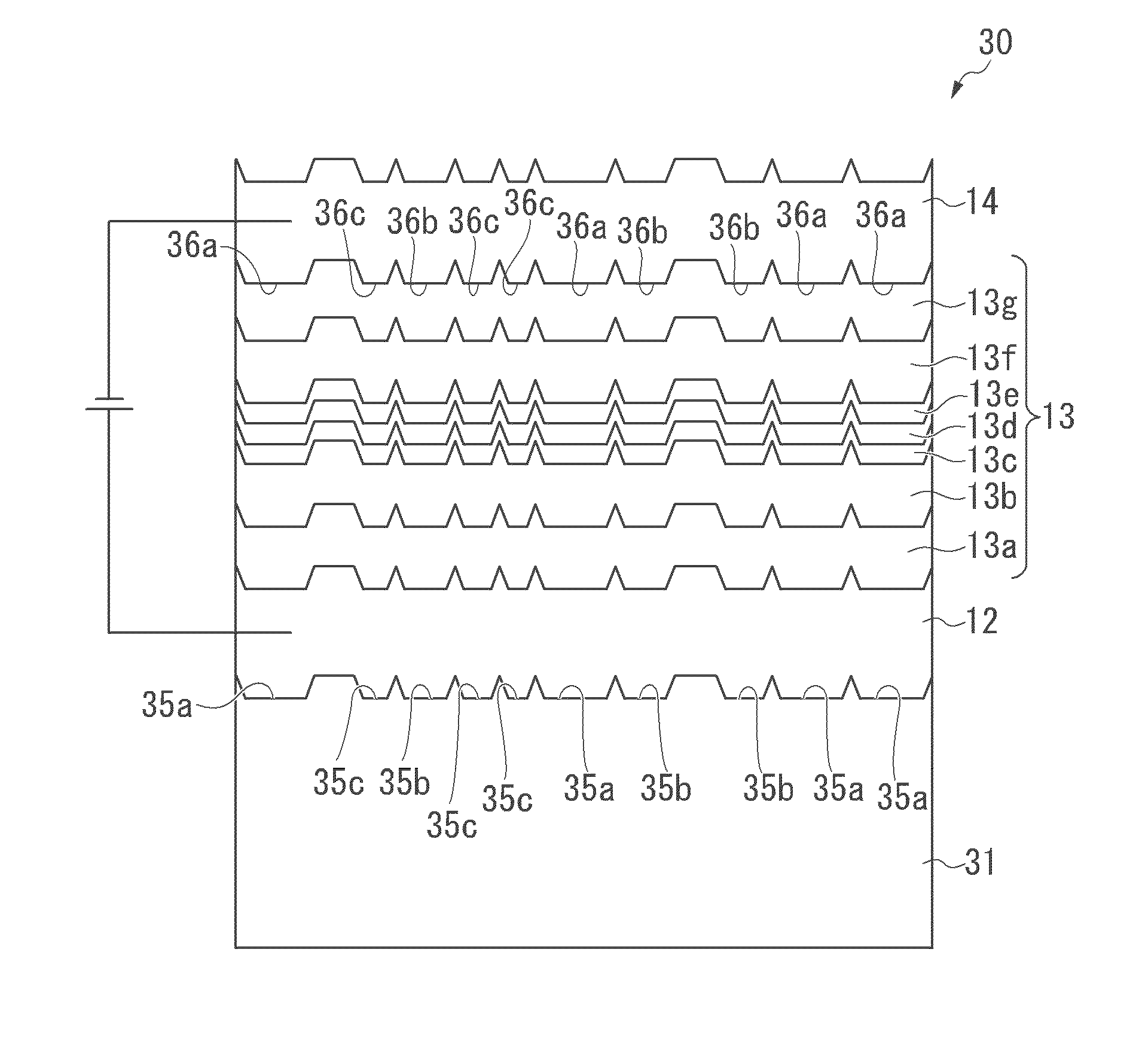
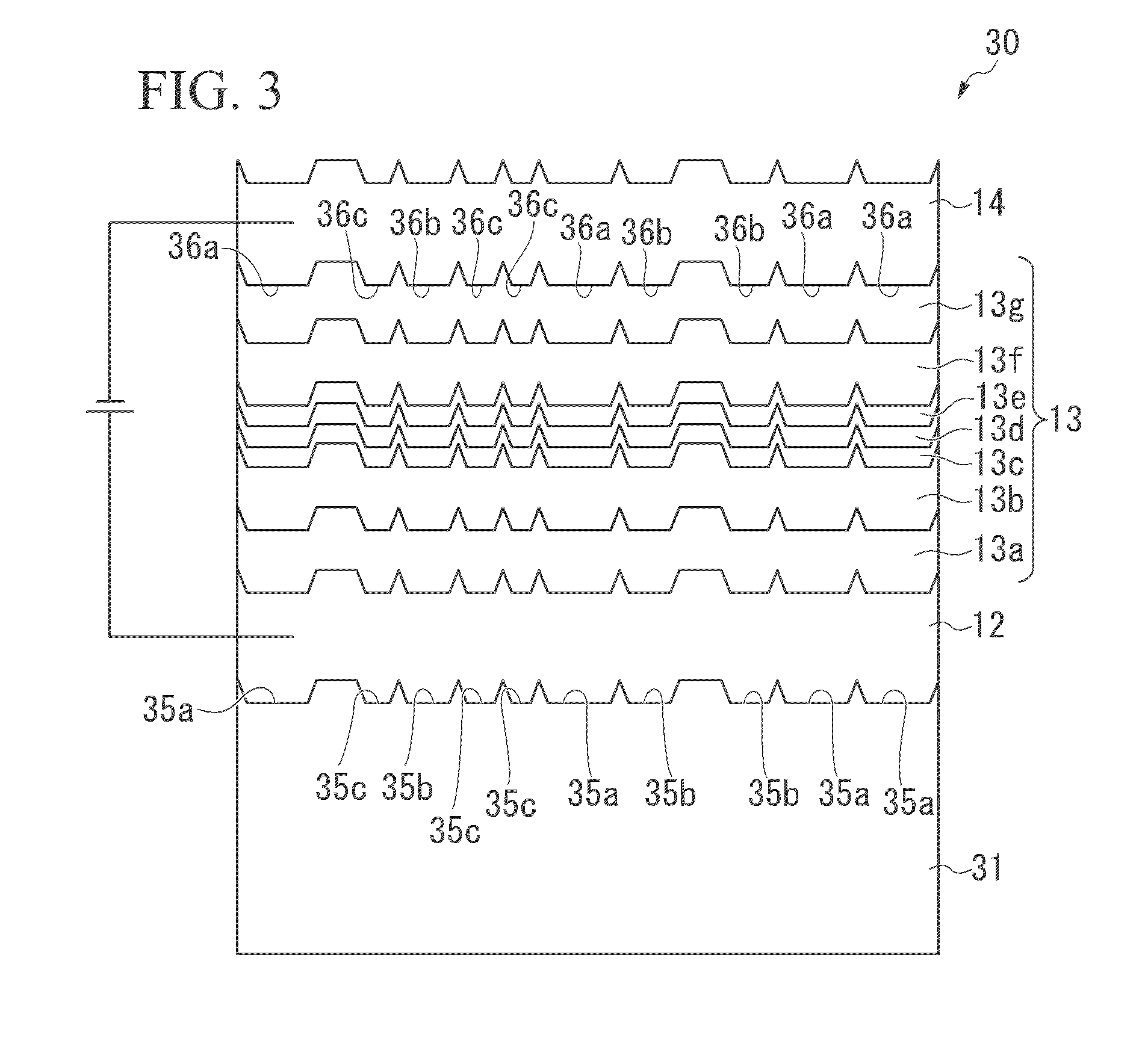
[0073]A schematic cross sectional view describing the structure of an organic light-emitting diode 10 manufactured using the present embodiment is illustrated in FIG. 1.

[0074]The organic light-emitting diode 10 is an organic light-emitting diode having a layer structure generally referred to as a bottom emission type structure, and has an anode conductive layer 12 formed from a transparent conductor, an EL layer 13, and a cathode conductive layer (metal layer) 14 formed from a metal stacked sequentially on top of a transparent substrate 11.

[0075]The surface of the transparent substrate 11 on the side that the anode conductive layer 12 is stacked is provided with an uneven structure in which a plurality of truncated cone-shaped convex portions 15a, 15b and 15c having mutually different diameters are arranged randomly in two dimensions. This uneven structure is described below in further detail.

[0076]The EL layer 13 is composed of a hole injection layer 13a, a hole transport layer 13b...

example 1

[0310]A 5.0% by mass aqueous dispersion (dispersed liquid) of a spherical colloidal silica having an average particle size A1 of 250.6 nm and a coefficient of variation of the particle size of 3.0%, a 5.0% by mass aqueous dispersion (dispersed liquid) of a spherical colloidal silica having an average particle size A2 of 150.1 nm and a coefficient of variation of the particle size of 7.4%, and a 5.0% by mass aqueous dispersion (dispersed liquid) of a spherical colloidal silica having an average particle size A3 of 90.2 nm and a coefficient of variation of the particle size of 9.4% were prepared. The average particle size and the coefficient of variation of the particle size were determined from the peak obtained by fitting the particle size distribution, determined by the particle dynamic light scattering method using a Zetasizer Nano-ZS manufactured by Malvern Instruments Ltd., to a Gaussian curve.

[0311]These three particle dispersions were each filtered through a membrane filter ha...

example 2

[0331]With the exception of using a mixture prepared by mixing a spherical colloidal silica having an average particle size A1 of 301.3 nm and a coefficient of variation of the particle size of 3.2%, a spherical colloidal silica having an average particle size A2 of 202.5 nm and a coefficient of variation of the particle size of 4.6%, and a spherical colloidal silica having an average particle size A3 of 90.2 nm and a coefficient of variation of the particle size of 9.4%, such that the occupied surface area ratio upon spreading the particles on the water surface was 1:1:1, exactly the same operations as Example 1 were used to coat the mixed particles onto the surface of a quartz substrate to prepare a quartz substrate having an uneven structure, and subsequently stack each of the electrode layers and the EL layer on the uneven structure using the same thicknesses and the same materials as Example 1, thus completing preparation of a bottom emission white organic light-emitting diode....


PUM


Abstract

A method of manufacturing an organic light-emitting diode including preparing, by a dry etching method using a particle single layer film as an etching mask, a substrate provided with an uneven structure in which a plurality of unevenness is arranged in two dimensions on the surface of the substrate, and stacking, on the uneven structure, at least an anode conductive layer, an EL layer including a light-emitting layer containing an organic light-emitting material, and a cathode conductive layer containing a metal layer, such that the uneven structure is reproduced on the surface of the metal layer on the side of the EL layer, wherein the particle single layer film is formed using a mixture of a plurality of particles having different particle sizes, and an uneven structure is provided which satisfies particular requirements.

Description

TECHNICAL FIELD[0001]The present invention relates to an organic light-emitting diode manufacturing method, an organic light-emitting diode, an image display device, an illumination device and a substrate.[0002]Priority is claimed on Japanese Patent Application No. 2011-147195, filed Jul. 1, 2011, the content of which is incorporated herein by reference.BACKGROUND ART[0003]Organic light-emitting diodes are light-emitting elements that use organic electroluminescence (hereafter, “electroluminescence” is abbreviated as “EL”), and generally have a structure in which conductive layers (an anode conductive layer and a cathode conductive layer) are provided on opposing surfaces of an EL layer containing a light-emitting layer which contains an organic light-emitting material. Besides the light-emitting layer, the EL layer may be provided with an electron transport layer or a hole transport layer or the like as required. Organic light-emitting diodes include bottom emission structures, in ...

Claims


Application Information

Patent Timeline
Patent Type & Authority Applications(United States)
IPC IPC(8): H01L51/56H01L51/52
CPCY10T428/24479H10K71/231H10K50/125H10K50/80H10K50/813H10K50/822H10K50/828H10K50/854H10K50/858H10K50/00H10K71/00H10K50/805H05B33/02H05B33/10
Inventor SHINOTSUKA, KEIOKAMOTO, TAKAYUKIKAWAMUKAI, ETSUKOYAMAMURA, NORIO
Owner OJI HLDG CORP
Why Eureka
Try Eureka