Super junction for semiconductor device and method for manufacturing the same

a semiconductor device and super junction technology, applied in the direction of semiconductor devices, electrical devices, transistors, etc., can solve the problems of difficult formation of trenches, process is sensitive to process tolerance (1%), and there is no way to fine-tune the

Active Publication Date: 2014-06-19
PFC DEVICE HLDG
View PDF3 Cites 7 Cited by
  • Summary
  • Abstract
  • Description
  • Claims
  • Application Information

AI Technical Summary

Benefits of technology

[0009]The object of the present invention is to provide a novel super junction structure for semiconductor device and method of manufacturing the same, the super junction structure has high aspect ratio and the semiconductor device using the super junction structure has high reverse voltage blockage.

Problems solved by technology

However, it is difficult to form trench with high aspect ratio on N type epitaxial layer 82.
Unfortunately, this process is very sensitive to process tolerance (<1%), which is not manufacturable for existing tool capability in epitaxial reactors and ion implanters.
Once ion implant and epitaxial growth are completed, there is no way to do fine tuning.

Method used


Image

  • Super junction for semiconductor device and method for manufacturing the same
  • Super junction for semiconductor device and method for manufacturing the same
  • Super junction for semiconductor device and method for manufacturing the same

Examples


first embodiment

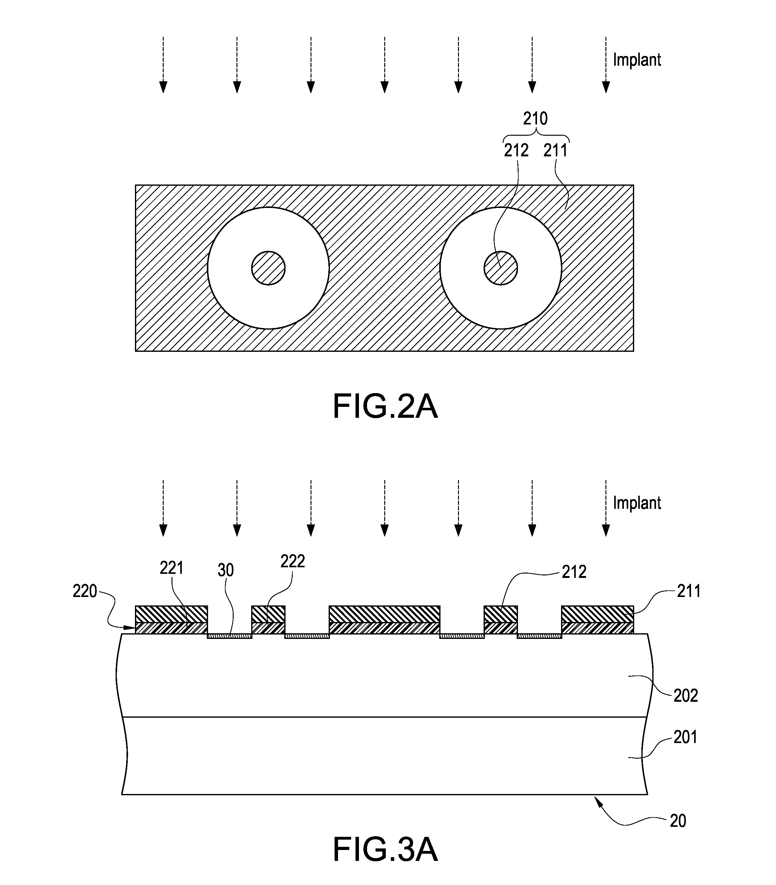
[0021]FIGS. 2A and 3A show the top view and section view for illustrating the first method of manufacturing super junction for semiconductor device according to the invention. As first shown in FIG. 3A, a semiconductor substrate 20 with a heavily-doped N-type silicon layer 201 (N+ silicon layer) and a lightly-doped N-type epitaxial layer 202 (N− epitaxial layer) is provided, where the lightly-doped N-type epitaxial layer 202 can be formed on top of the semiconductor substrate 20 by epitaxial process. The drawing is not sketched to the dimensions. Even the lightly-doped N-type epitaxial layer 202 is shown to be thicker than the heavily-doped N-type silicon layer 201, it should be noted the drawing is only for demonstration and the lightly-doped N-type epitaxial layer 202 is actually thinner than the heavily-doped N-type silicon layer 201. Then, a bottom mask layer (not labeled, for example an LTO (Low Temperature Oxide) layer) is grown on the substrate 20 by Low Pressure Chemical Vap...

second embodiment

[0029]FIGS. 4A and 5A show the top view and cross section view of middle cut line horizontally for illustrating the second method of manufacturing super junction for semiconductor device according to the invention. As first shown in FIG. 5A, a semiconductor substrate 20 with a heavily-doped N-type siliconlayer 201 (N+ silicon layer) and a lightly-doped N-type epitaxial layer 202 (N− epitaxial layer) is provided. Even the lightly-doped N-type epitaxial layer 202 is shown to be thicker than the heavily-doped N-type silicon layer 201, it should be noted the draw s only for demonstration and the lightly-doped N-type epitaxial layer 202 is actually thinner than the heavily-doped N-type silicon layer 201. Then, a mask layer (not labeled, for example an LTO (Low Temperature Oxide) layer) is grown on the substrate 20 by Low Pressure Chemical Vapor Deposition process. Then, a first photoresist layer 210 is formed on the mask layer. As shown in FIGS. 4A and 5A, the first photoresist layer 210...

third embodiment

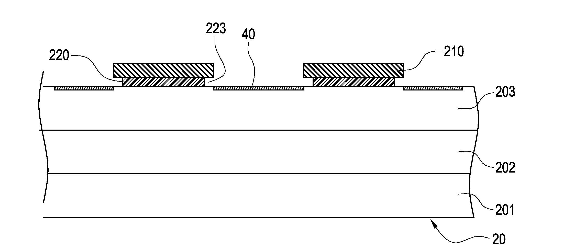
[0036]FIGS. 6A and 7A show the top view and cross section view of middle cut line horizontally for illustrating the third method of manufacturing super junction for semiconductor device according to the invention. As first, shown in FIG. 7A, a semiconductor substrate 20 with a heavily-doped N-type silicon layer 201 (N+ silicon layer) and a lightly-doped N-type epitaxial layer 202 (N− epitaxial layer) are provided. Then a lightly-doped P type epitaxial process is conducted to form a lightly-doped P type epitaxial layer 203 on the lightly-doped N-type epitaxial layer 202. Afterward, a bottom mask layer (not labeled, for example an LTO (Low Temperature Oxide) layer) is grown on the lightly-doped P type epitaxial layer 203 by Low Pressure Chemical Vapor Deposition process. Then, a first photoresist layer 210 functioned as a top mask layer is formed on the bottom mask layer.

[0037]As shown in FIGS. 6A, the first photoresist layer 210 defines a circular layer (not labeled). It should be no...


PUM


Abstract

A super junction for semiconductor device includes a silicon substrate with a first conductive type epitaxial layer, a plurality of highly-doped second conductive type columns formed in the first conductive type epitaxial layer, and a plurality of lightly-doped (first conductive type or second conductive type) side walls formed on outer surfaces of the highly-doped second conductive type. The semiconductor device is super-junction MOSFET, super junction MOSFET, super junction Schottky rectifier, super junction IGBT, thyristor or super junction diode.

Description

BACKGROUND OF THE INVENTION[0001]1. Field of the Invention[0002]The present invention relates to a semiconductor structure and a method for manufacturing the same, especially to a super junction for semiconductor device and a method for manufacturing the same.[0003]2. Description of Related Art[0004]Since the first introduction by Dr. Chen in 1991, super junction devices are under substantive research for improved performance.[0005]For example, U.S. Pat. No. 6,608,350 was disclosed with a trench type super junction device. FIG. 1 shows the sectional view of the trench type super junction device in U.S. Pat. No. 6,608,350. The trench type super junction MOS device comprises a substrate 81, an N type epitaxial layer 82, a plurality of parallel trenches 83, P type layer 84 on sidewall of each trench 83, P base 93 on the N type epitaxial layer 82, gate oxide layer 87 and gate 88 between two adjacent trenches 83 and atop the N type epitaxial layer 82, source 89 and source electrode 91 at...

Claims


Application Information

Patent Timeline
Patent Type & Authority Applications(United States)
IPC IPC(8): H01L29/06
CPCH01L29/0619H01L29/0634H01L21/26513H01L21/266H01L21/324H01L29/0878H01L29/66136H01L29/66143H01L29/66333H01L29/66363H01L29/66712H01L29/7393H01L29/74H01L29/749H01L29/7802H01L29/861H01L29/872
Inventor CHANG, PAUL CHUNG-CHENCHAO, KUO-LIANGCHEN, MEI-LINGKAO, LUNG-CHING
Owner PFC DEVICE HLDG
Why Eureka
Try Eureka