Adjustable pole and zero location for a second order low pass path filter used in a phase lock loop circuit

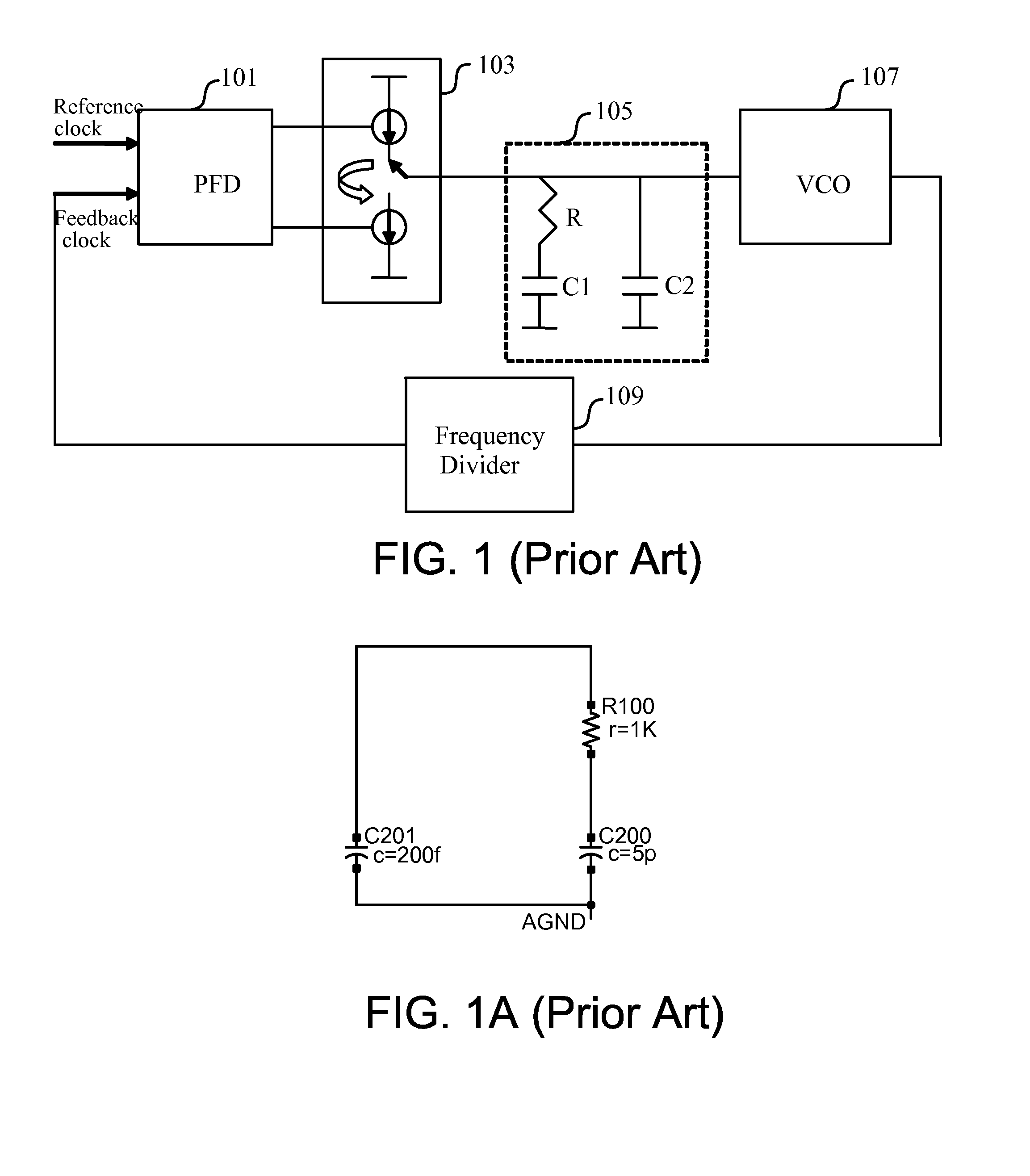
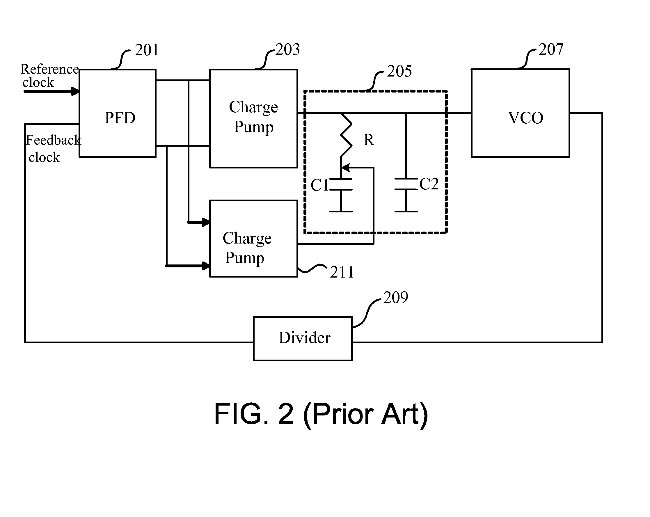
a phase lock loop and low-pass path filter technology, applied in the field of circuit design technology, can solve the problems of many packaging inconvenience in ic chip applications, large on-die capacitors that are impossible to bear, and the disadvantage of the phase lock loop in fig. 2, and achieve the effect of small on-die area, low bandwidth pll, and increased effective capacitan

Inactive Publication Date: 2014-07-03
DANG YEN
View PDF0 Cites 2 Cited by
  • Summary
  • Abstract
  • Description
  • Claims
  • Application Information

AI Technical Summary

Benefits of technology

[0011]The present invention is directed to a Phase Lock Loop circuit that includes a loop filter capable of tuning loop zero and pole frequency by adjusting the gain of the amplifier. This invention also has an advantage to provide small on-die area particularly related to the loop filter in the PLL circuit. In particular, embodiments also provide methods for IC designers to use this loop filter for adjusting the pole and zero location of the PLL which affects the bandwidth. The pole and zero location are controlled by an amplifier and some on-chip R, C components within the loop filter. The effective capacitance will be magnified by the gain of the amplifier. The advantage of the filter device and the method according to embodiments of the present invention provides a much superior way to achieve a low bandwidth PLL without using a huge on-die capacitor.
[0013]In another specific embodiment, the present invention provides a loop filter capable of tuning pole location and reducing bandwidth in a PLL circuit. The loop filter includes a resistor, a first capacitor, three second capacitors having a same capacitance value, an amplifier having a tunable gain, a first switch and a second switch, and a DC bias circuit. The first capacitor forms a dominant pole of the loop circuit. The resistor is coupled the first capacitor, deciding the zero frequency. A combination of the amplifier, the first capacitor, and the resistor forms a feedback circuit that can shift the pole location by changing the gain of the amplifier. In an embodiment, due to the Miller effect, an effective capacitance value of the first capacitor is magnified by the gain of the amplifier which is a differential amplifier with two input terminals and one output terminal. DC bias voltages of the two input terminals are set up by the first switch and the second switch respectively via a DC bias circuit. During an operation of the PLL circuit, the DC bias voltages of the two input terminals of the amplifier remain the same and un-changed even a DC voltage at an input node of the loop filter varies, allowing the amplifier to operate in a fixed DC operating point with the gain tunable up to 40 dB to 80 dB. Both the first switch and the second switch turn on when a reference clock is at ground voltage and turn off when the reference clock is at high voltage. AC input signals for the amplifier are coupled from the three second capacitors which are coupled to an output node of a charge pump which is also the input node of the loop filter. The amplifier is coupled with the first capacitor to form a Miller capacitor, effectively increasing the capacitor value by the gain of the amplifier and thus reducing the bandwidth of the PLL circuit.

Problems solved by technology

However, for such a low bandwidth, it requires a huge on die capacitor that is impossible to bear.
The area of C1 is very big in order to have a lower frequency zero, resulting in many packaging inconvenience in IC chip applications.
However, the Phase Lock Loop in FIG. 2 has a disadvantage.
Mismatch between the two charge pumps limits the effectiveness of the circuit.
This structure has some inherit problems.
Third, this device is a single stage single input amplifier with very limited gain K, for example, K is normally just around 10 or so.

Method used


Image

  • Adjustable pole and zero location for a second order low pass path filter used in a phase lock loop circuit
  • Adjustable pole and zero location for a second order low pass path filter used in a phase lock loop circuit
  • Adjustable pole and zero location for a second order low pass path filter used in a phase lock loop circuit

Examples


Embodiment Construction

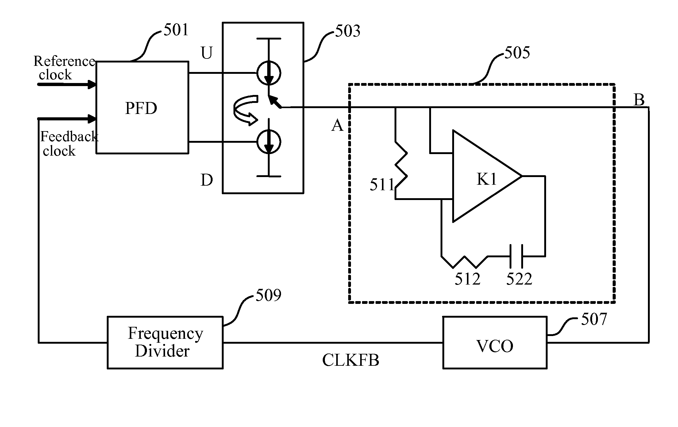
[0032]The present invention relates generally to circuit design technology. More particularly, the present invention provides a circuit structure functioning as a filter device capable of tuning loop zero and pole frequency by adjusting the gain of an amplifier. Merely by way of example, the present filter device is applicable in phase lock loop circuit characterized by adjustable pole and zero locations with reduced real estate for superior low-bandwidth application, but it would be recognized that the invention may have many other integrated circuit applications.

[0033]Embodiments of this invention provide a loop filter device and a method for IC designers to adjust the pole and zero location in the phase lock loop (PLL) circuit which affects the bandwidth. The pole and zero location are tuned by an amplifier and some on-chip resistor R, capacitor C components associated with the loop filter device. The effective capacitance can be magnified by the gain of the amplifier. The advant...


PUM


Abstract

This invention provides a loop filter device and a method for IC designers to adjust the pole or zero location of a phase lock loop (PLL) circuit. The pole and zero location are controlled by an amplifier and some on-chip resistor and capacitor components. The effective capacitance is magnified by the gain of the amplifier. The advantage of the loop filter device and the method according to embodiments of the present invention provides a feasible way to achieve a very low bandwidth in the PLL circuit without a huge external surface-mount capacitor.

Description

CROSS-REFERENCES TO RELATED APPLICATIONS[0001]This application is a divisional application of U.S. patent application Ser. No. 13 / 666,120, filed Nov. 1, 2012 by Yen Dang, and claims priority to U.S. provisional application no. 61 / 554,028, filed Nov. 1, 2011, by Yen Dang, and hereby incorporated by reference in its entirety herein for all purposes.BACKGROUND OF THE INVENTION[0002]The present invention relates generally to circuit design technology. More particularly, the present invention provides a circuit structure functioning as a filter device capable of tuning loop zero and pole frequency by adjusting the gain of an amplifier. Merely by way of example, the present filter device is applicable in phase lock loop circuit characterized by tunable pole and zero locations with reduced on-die real estate for superior low-bandwidth application, but it would be recognized that the invention may have many other integrated circuit applications.[0003]In modern integrated circuit (IC) chip d...

Claims


Application Information

Patent Timeline
Patent Type & Authority Applications(United States)
IPC IPC(8): H03H11/12H03L7/093
CPCH03H11/1269H03L7/093H03L7/085
Inventor DANG, YEN
Owner DANG YEN
Why Eureka
Try Eureka