Organic Light-Emitting Device Having Improved Efficiency Characteristics and Organic Light-Emitting Display Apparatus Including the Same

a technology of efficiency characteristics and light-emitting display apparatus, which is applied in the direction of organic semiconductor devices, luminescent compositions, thermoelectric devices, etc., can solve the problems of low luminescent efficiency characteristics of organic light-emitting devices using phosphorescent materials, and achieve low luminescent efficiency, high luminescent efficiency, and high brightness. region

Active Publication Date: 2014-07-10
SAMSUNG DISPLAY CO LTD
View PDF11 Cites 60 Cited by
  • Summary
  • Abstract
  • Description
  • Claims
  • Application Information

AI Technical Summary

Benefits of technology

[0010]According to embodiments of the present invention, an organic light-emitting device includes a phosphorescent materi...

Problems solved by technology

However, even when these methods are used, the low brightness efficiency characterist...

Method used


Image

  • Organic Light-Emitting Device Having Improved Efficiency Characteristics and Organic Light-Emitting Display Apparatus Including the Same
  • Organic Light-Emitting Device Having Improved Efficiency Characteristics and Organic Light-Emitting Display Apparatus Including the Same
  • Organic Light-Emitting Device Having Improved Efficiency Characteristics and Organic Light-Emitting Display Apparatus Including the Same

Examples


example 1

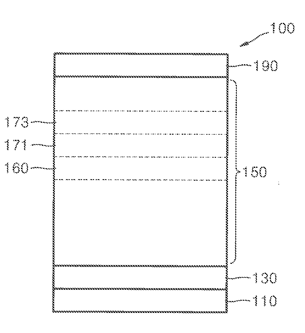
[0181]An anode was prepared by cutting an ITO(7 nm) / Ag(100 nm) / ITO(7 nm) substrate (manufactured by Samsung mobile display (SMD) Co., Ltd using glass manufactured by Corning Company) to a size of 50 mm×50 mm×0.7 mm, ultrasonically cleaning the glass substrate using isopropyl alcohol and pure water for 30 minutes each, and then irradiating with UV light for 10 minutes and exposing to ozone to clean. Then, the anode was loaded into a vacuum deposition apparatus.

[0182]Compound 301 was vacuum deposited on the glass substrate to form a hole injection layer having a thickness of 750 Å, and then Compound 311 was vacuum deposited on the hole injection layer to form a hole transportation layer having a thickness of 1300 Å.

[0183]Compound 507 as a host and Compound 401 as a phosphorescent dopant were co-deposited at a weight ratio of 98:2 on the hole transportation layer to form a red emission layer having a thickness of 400 Å.

[0184]Subsequently, Compound 1 and Compound 401 were vacuum deposit...

example 2

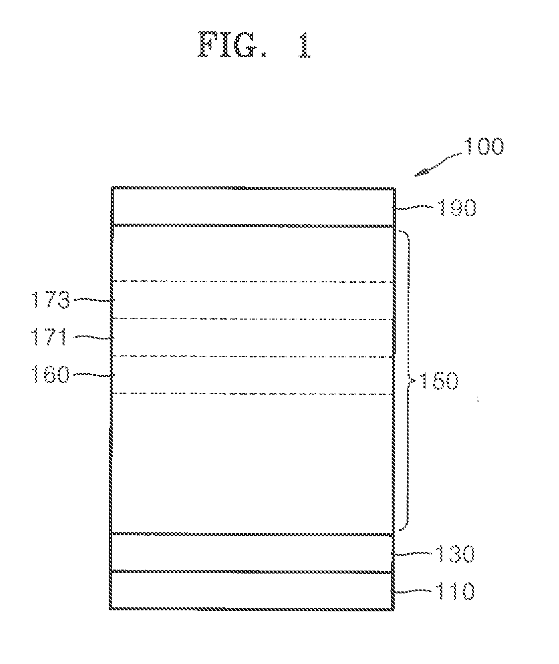
[0187]An organic light-emitting device was manufactured as in Example 1, except that the electron control layer was formed to a thickness of 100 Å instead of 50 Å.

example 3

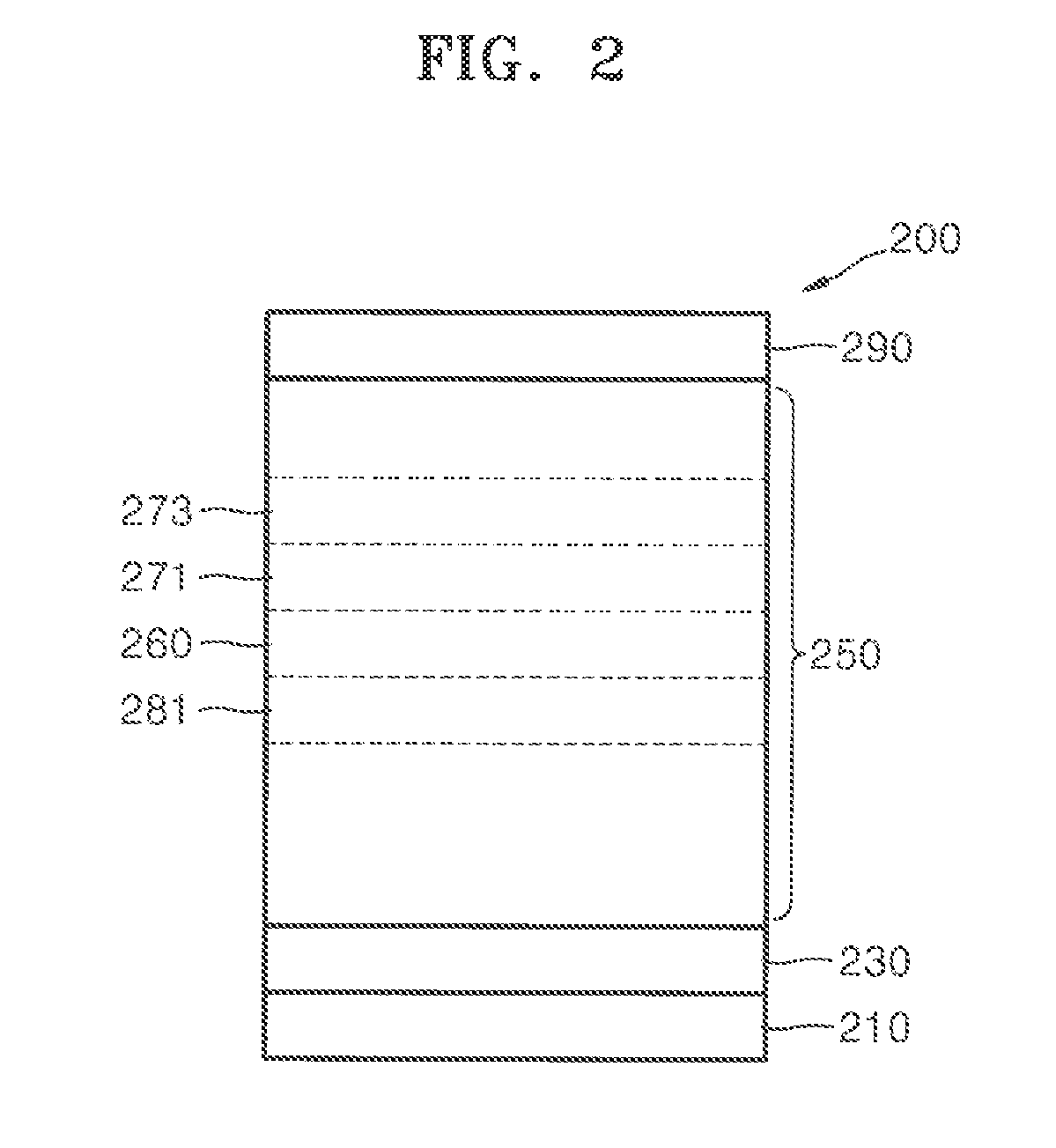
[0188]An organic light-emitting device was manufactured as in Example 1, except that the electron control layer was formed to a thickness of 100 Å instead of 50 Å, and a second electron control layer having a thickness of 100 Å and formed of only Compound 1 was additionally formed on the first electron control layer.


PUM


Abstract

An organic light-emitting device includes: a first electrode, a second electrode facing the first electrode, a phosphorescent emission layer between the first electrode and the second electrode, an electron transportation layer between the phosphorescent emission layer and the second electrode, an electron control layer between the phosphorescent emission layer and the electron transportation layer, and an electron blocking layer between the phosphorescent emission layer and the first electrode. An organic light-emitting display apparatus includes the organic light-emitting device.

Description

CROSS-REFERENCE TO RELATED PATENT APPLICATION[0001]This application claims priority to and the benefit of Korean Patent Application No. 10-2013-0001210, filed on Jan. 4, 2013 in the Korean Intellectual Property Office, the entire content of which is incorporated herein by reference.BACKGROUND[0002]1. Technical Field[0003]Embodiments of the present invention relate to an organic light-emitting device with improved efficiency characteristics, and in particular, to an organic light-emitting device with improved luminescent efficiency characteristics with respect to brightness, and an organic light-emitting display apparatus with improved luminescent efficiency characteristics in a black state due to the inclusion of the organic light-emitting device.[0004]2. Description of the Related Art[0005]Organic light-emitting devices (OLEDs) are self-emitting devices having advantages such as wide viewing angles, good contrast, quick response speeds, high brightness, and good driving voltage cha...

Claims


Application Information

Patent Timeline
IPC IPC(8): H01L51/00
CPCC09K11/06H01L51/0052H01L51/0061H01L51/0085H01L51/0087H01L51/0072H01L2251/558H01L51/50H01L51/5004H01L51/5016H01L51/5072H01L51/5096H01L51/0058C09K2211/185H10K85/615H10K85/626H10K85/636H10K85/6572H10K85/346H10K85/342H10K50/00H10K50/11H10K2101/40H10K2101/10H10K50/16H10K50/18H10K2102/351H10K50/12
Inventor CHO, HWAN-HEE
Owner SAMSUNG DISPLAY CO LTD
Why Eureka
Try Eureka