Method and Apparatus for Optical Waveguide-to-Semiconductor Coupling and Optical Vias for Monolithically Integrated Electronic and Photonic Circuits

a monolithic integrated electronic and photonic circuit technology, applied in the field of integrated circuits, can solve the problems of waveguide further, low index-contrast system, and inability to attract small beams of a few microns or tens of microns in diameter

Active Publication Date: 2014-07-10
MASSACHUSETTS INST OF TECH +1
View PDF39 Cites 71 Cited by
  • Summary
  • Abstract
  • Description
  • Claims
  • Application Information

AI Technical Summary

Problems solved by technology

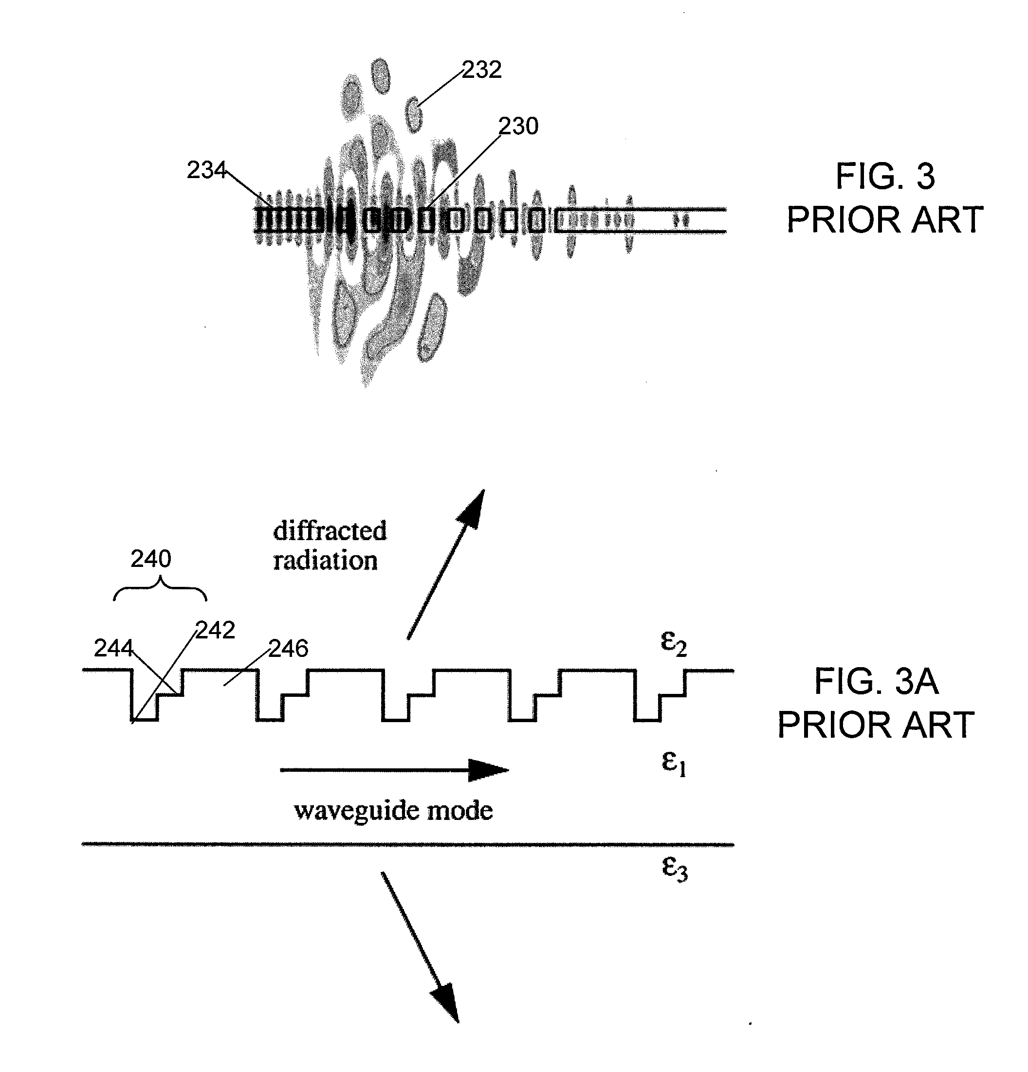
If only one receiver is placed either above, or below, but not on both sides of the coupler, then the bidirectional radiation is a source of substantial optical loss as uncollected light radiates away from the opposite side of the coupler.
Hence, low index-contrast systems may not be suitable for exciting small beams of a few microns or tens of microns in diameter, especially as suitable for coupling to standard 10 micron-diameter core telecom optical fiber, or small core (e.g. 5 micron diameter) fibers, or for short-hop optical vias of optimal design, which call for small diameter beams as discussed later in the disclosure.
Furthermore, out-of-plane confinement of the light in the waveguide further reduces the effective index.
Because of the length and weak strengths of both gratings, the MFDs of these embodiments are too large for most efficient coupling with a standard single-mode fiber because such fibers typically have a 10 micron mode field diameter.
Another consequence of strong coupling in high contrast gratings is substantial reflection per tooth, where perturbative approaches to model the grating begin to fail.
Thus, the latter case is a worse approximation of scattering power from a guided slab mode and will produce larger radiative losses.
This occurs because the desired grating strength for a Gaussian beam is too large, and the largest grating strength achievable with the example grating is not large enough.
The resulting grating is non-uniform because it radiates at a non-uniform rate along the grating to form the Gaussian beam shape.
The pri

Method used


Image

  • Method and Apparatus for Optical Waveguide-to-Semiconductor Coupling and Optical Vias for Monolithically Integrated Electronic and Photonic Circuits
  • Method and Apparatus for Optical Waveguide-to-Semiconductor Coupling and Optical Vias for Monolithically Integrated Electronic and Photonic Circuits
  • Method and Apparatus for Optical Waveguide-to-Semiconductor Coupling and Optical Vias for Monolithically Integrated Electronic and Photonic Circuits

Examples


Embodiment Construction

[0050]Microelectronics relies on carefully optimized complementary metal oxide semiconductor (CMOS) processes. In this document, we will refer to a CMOS process including silicon on insulator (SOI) CMOS and bulk silicon CMOS (“bulk CMOS”) variants. We will refer to SOI CMOS and bulk CMOS processes designed for microelectronics as transistor processes, in contrast to custom photonics processes that are typically tailored for photonics and do not support high performance transistors. Examples of SOI CMOS transistor processes include 45 nm SOI CMOS process supported by IBM's 12SOI (IBM, Armonk, N.Y.), as well as by GlobalFoundries (Sunnyvale, Calif.), 32 nm SOI CMOS (IBM 32SOI process), and many others in the semiconductor industry. Although silicon photonics is sometimes referred to as “CMOS compatible” in the literature, this typically refers to using silicon or CMOS compatible materials, and -not- to compatibility of devices with a standard CMOS transistor process. In this disclosur...


PUM


Abstract

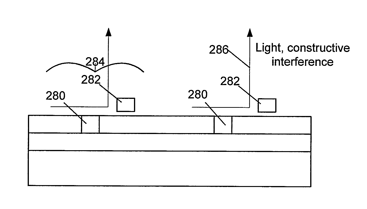
An optical coupler has a waveguide coupled to a grating of multiple scattering units, each scattering unit having a first scattering element formed of a shape in a polysilicon gate layer and a second scattering element formed of a shape in a body silicon layer of a metal-oxide-semiconductor (MOS) integrated circuit (IC). The couplers may be used in a system having a coupler on each of a first and second IC, infrared light being formed into a beam passing between the couplers. Vias may be interposed in third ICs between the first and second ICs. The couplers may be configured with nonuniform width of scattering elements to produce Gaussian or focused beams.

Description

RELATED APPLICATIONS AND CLAIM TO PRIORITY[0001]This application claims priority from U.S. Provisional Patent Application 61 / 751,187 filed 10 Jan. 2013, the entire contents of which is hereby incorporated herein by reference.GOVERNMENT INTEREST[0002]This invention was made with government support under grant number HR0011-11-C-0100 awarded by DOD / DARPA, and Grant number ECCS1128709 awarded by National Science Foundation. The government has certain rights in the invention.TECHNICAL FIELD[0003]The present document relates to the field of integrated circuits having integrated optical devices and, in many embodiments, electronic devices on the same die. In particular embodiments, the integrated optical devices include optical waveguides and other optical components on a same die as CMOS circuitry.BACKGROUND[0004]There are many applications, including cameras, optical data transmitters, and optical data receivers, where electronic circuitry and optical devices are combined on a single in...

Claims


Application Information

Patent Timeline
IPC IPC(8): G02B6/34
CPCG02B6/34G02B6/124
Inventor POPOVIC, MILOS
Owner MASSACHUSETTS INST OF TECH
Why Eureka
Try Eureka