Nonvolatile memory element, nonvolatile memory device, nonvolatile memory element manufacturing method, and nonvolatile memory device manufacturing method

a technology of nonvolatile memory and manufacturing method, which is applied in the direction of bulk negative resistance effect devices, semiconductor devices, electrical devices, etc., can solve the problem of limiting the miniaturization of existing flash memories using floating gates, and achieve the reduction of maximum area, increase current flow density, and reduce the leak current of variable resistance layers

Active Publication Date: 2014-07-17
PANASONIC SEMICON SOLUTIONS CO LTD
View PDF9 Cites 33 Cited by
  • Summary
  • Abstract
  • Description
  • Claims
  • Application Information

AI Technical Summary

Benefits of technology

[0014]The nonvolatile memory element according to the aspect of the present invention allows the third metal oxide to decrease the maximum area of the second metal oxide in a planar direction, that is, a direction crossing a direction of drive current flowing to the nonvolatile memory element, to reduce leak current of the variable resistance layer and increase a density of current flowing to the first metal oxide. This makes it possible to easily form a conductive path in the first metal oxide and reduce the initial breakdown voltage, and thus it is possible to initialize the element at low voltage.
[0015]At the same time, by covering the side walls of the third metal oxide with the side wall protecting layer, it is possible to suppress a deterioration and increasing fluctuation in resistance characteristics of the nonvolatile memory element which are caused by supply of oxygen to the third metal oxide and further oxidation of the third metal oxide due to a deposition step and a heat treatment step for an interlayer insulating layer in a manufacturing process after formation of the nonvolatile memory element, or by an increasing fluctuation in an oxidation layer including the third metal oxide.
[0016]These features significantly contribute to particularly the miniaturization and the increase in capacity of memories.

Problems solved by technology

In response to such a demand, it is said that there is a limit on the miniaturization of existing flash memories using floating gates.

Method used


Image

  • Nonvolatile memory element, nonvolatile memory device, nonvolatile memory element manufacturing method, and nonvolatile memory device manufacturing method
  • Nonvolatile memory element, nonvolatile memory device, nonvolatile memory element manufacturing method, and nonvolatile memory device manufacturing method
  • Nonvolatile memory element, nonvolatile memory device, nonvolatile memory element manufacturing method, and nonvolatile memory device manufacturing method

Examples


embodiment 1

Modification of Embodiment 1

[0187]A nonvolatile memory element of which endurance characteristics are enhanced is described as a nonvolatile memory element according to a modification of Embodiment 1.

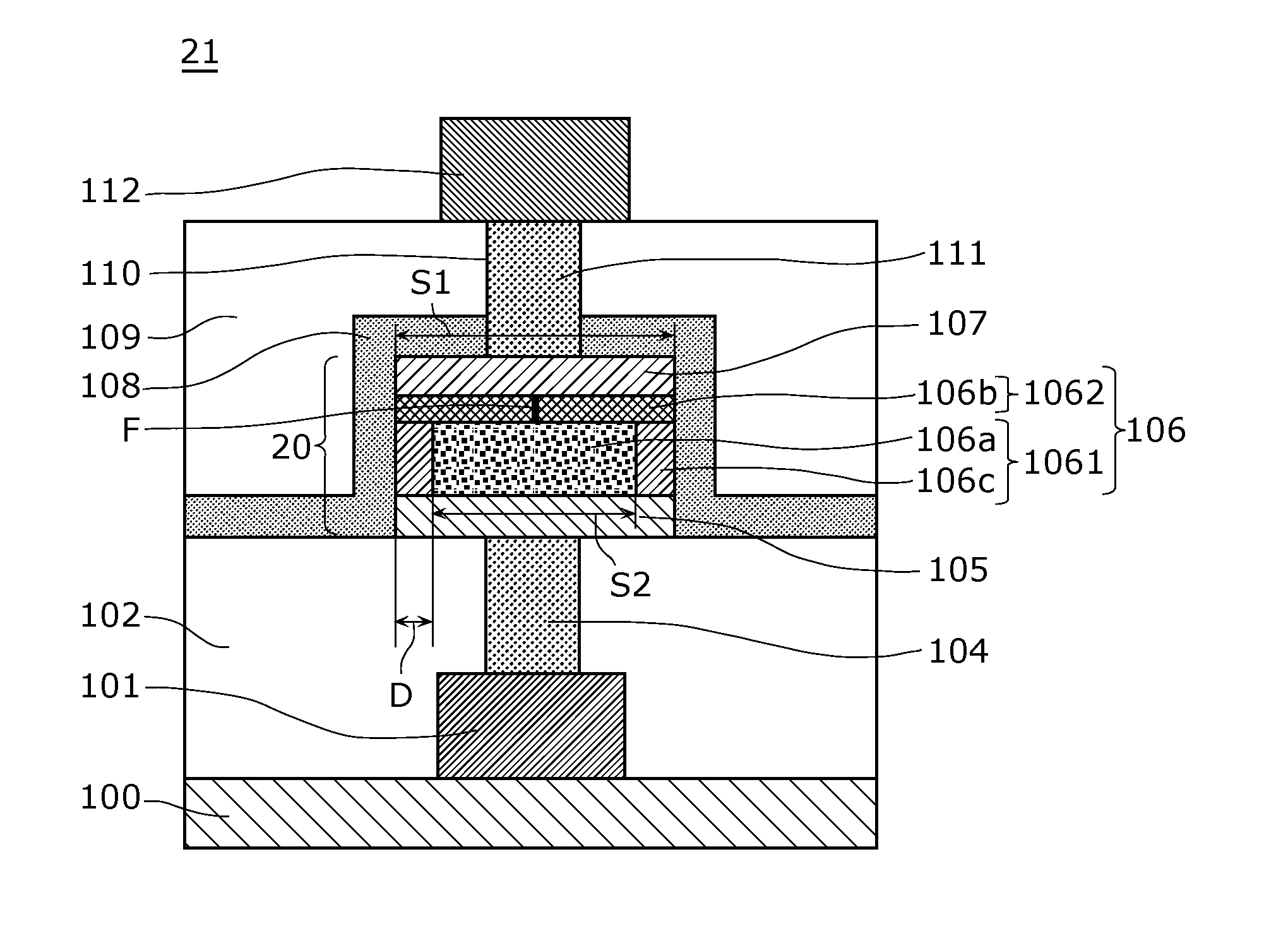
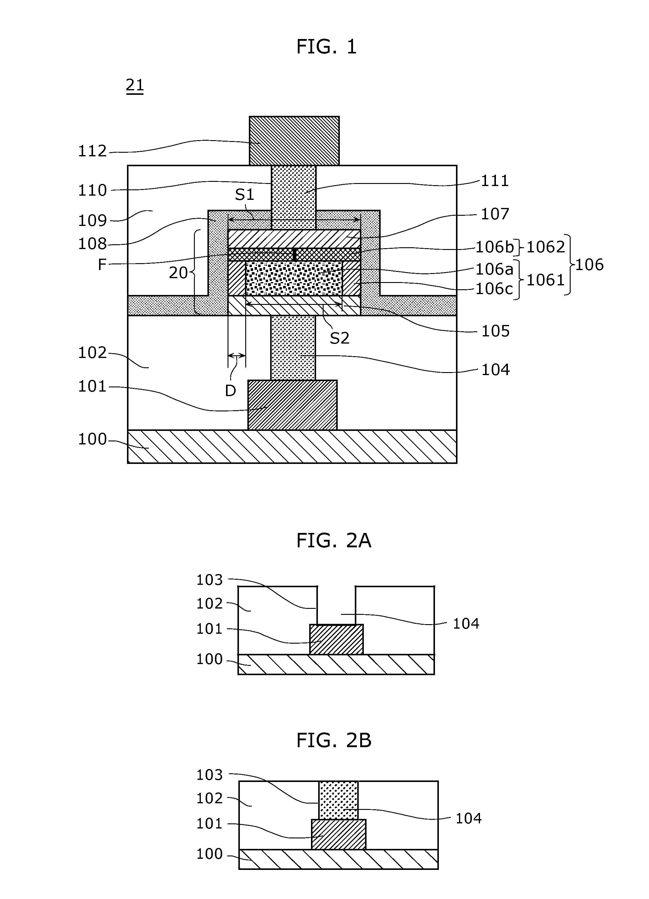
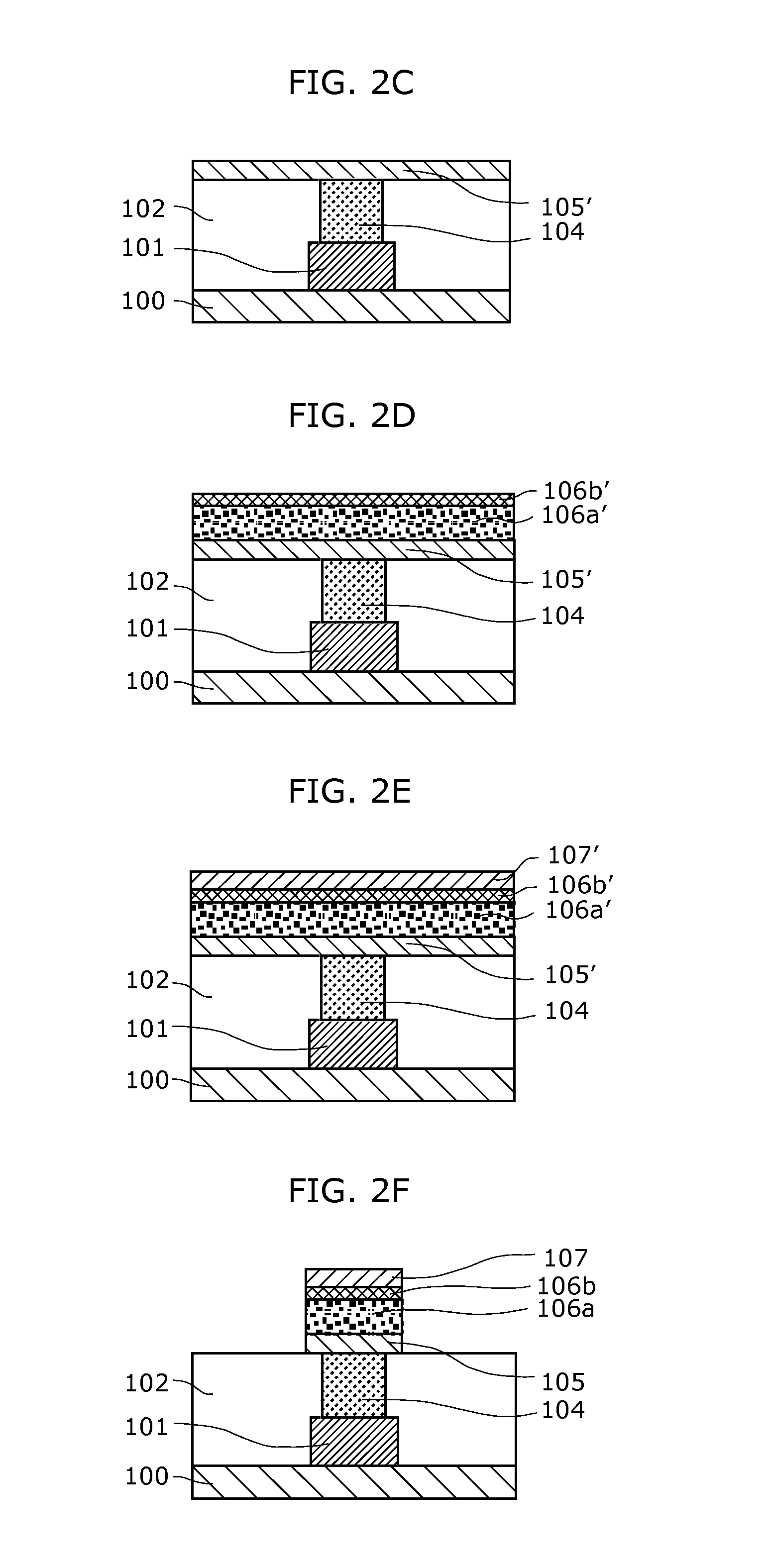
[0188]FIG. 10 is a cross-sectional view illustrating an exemplary structure of a nonvolatile memory device 25 including a nonvolatile memory element 24 according to the modification of Embodiment 1.

[0189]In the nonvolatile memory element 24, a first metal oxide 106a included in a variable resistance layer 117 has a laminated structure of metal oxides having different oxygen deficiencies, and includes as layers a first region 106a1 connected to a first electrode 105 and a second region 106a connected to a second variable resistance layer 1062.

[0190]A second region 106a2 of the first metal oxide 106a has an oxygen deficiency lower than that of the first region 106a1 of the first metal oxide 106a and higher than that of a second metal oxide 106b.

[0191]In other words, the variable resistan...

embodiment 2

[0202]FIG. 12 is a cross-sectional view illustrating an exemplary structure of a nonvolatile memory device according to Embodiment 2 of the present invention. A nonvolatile memory element 30 according to this embodiment differs from the example illustrated in FIG. 3 in that a side wall protecting layer 118 covers only the sides of the first electrode 105, the variable resistance layer 106, and the second electrode 107. Stated differently, the nonvolatile memory element 30 illustrated in FIG. 12 has a side wall structure such that the side wall protecting layer 118 covers only the side wall portions of the nonvolatile memory element 30. In Embodiment 1, since it is necessary to process, by dry etching, the two-layered film of the second interlayer insulating layer 109 and the side wall protecting layer 108 having different selection ratios when the contact hole 110 is formed, there is a fear for an addition of an etching step, a stability of a contact resistance value, or the like. I...


PUM

PropertyMeasurementUnit
thicknessaaaaaaaaaa
resistivityaaaaaaaaaa
thicknessaaaaaaaaaa

Abstract

A nonvolatile memory element including: a first electrode; a second electrode; a variable resistance layer that is between the first electrode and the second electrode and includes, as stacked layers, a first variable resistance layer connected to the first electrode and a second variable resistance layer connected to the second electrode; and a side wall protecting layer that has oxygen barrier properties and covers a side surface of the variable resistance layer. The first variable resistance layer includes a first metal oxide and a third metal oxide formed around the first metal oxide and having an oxygen deficiency lower than that of the first metal oxide, and the second variable resistance layer includes a second metal oxide having an oxygen deficiency lower than that of the first metal oxide.

Description

TECHNICAL FIELD[0001]The present invention relates to a variable resistance nonvolatile memory element of which a resistance value changes with an application of electric pulses, and to a nonvolatile memory device including the variable resistance nonvolatile memory element.BACKGROUND ART[0002]In recent years, along with development of the digital technology, electronic devices such as portable information devices and information home appliances have increasingly higher-level functionalities. There is thus a higher demand on nonvolatile memory elements for an increase in capacity, a reduction in power for writing, an increase in speed for writing / reading, and a longer operating life.[0003]In response to such a demand, it is said that there is a limit on the miniaturization of existing flash memories using floating gates. On the other hand, a nonvolatile memory element (i.e., a variable resistance memory) using a variable resistance layer as a material of a memory unit can be compose...

Claims


Application Information

Patent Timeline
Patent Type & Authority Applications(United States)
IPC IPC(8): H01L45/00
CPCH01L45/1608H01L45/145H10B63/20H10B63/30H10B63/84H10N70/24H10N70/828H10N70/026H10N70/826H10N70/8833H10N70/063H10N70/8265H10N70/021H10N70/883
Inventor YONEDA, SHINICHIMIKAWA, TAKUMIITO, SATORUHAYAKAWA, YUKIOHIMENO, ATSUSHI
Owner PANASONIC SEMICON SOLUTIONS CO LTD
Why Eureka
Try Eureka