Material for organic optoelectronic device, organic light emitting diode including the same, and display including the organic light emitting diode

Active Publication Date: 2014-07-17
SAMSUNG ELECTRONICS CO LTD +1
View PDF3 Cites 178 Cited by
  • Summary
  • Abstract
  • Description
  • Claims
  • Application Information

AI Technical Summary

Benefits of technology

[0021]A material for an organic optoelectronic device that may provide an organic op

Problems solved by technology

However, development of an organic material layer forming material for an organic light emitting

Method used


Image

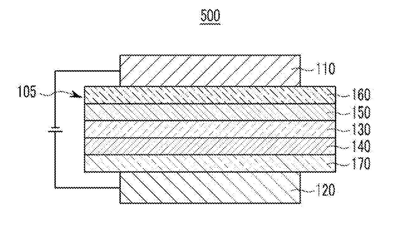
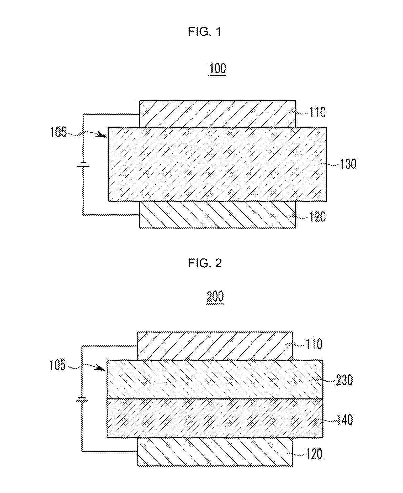
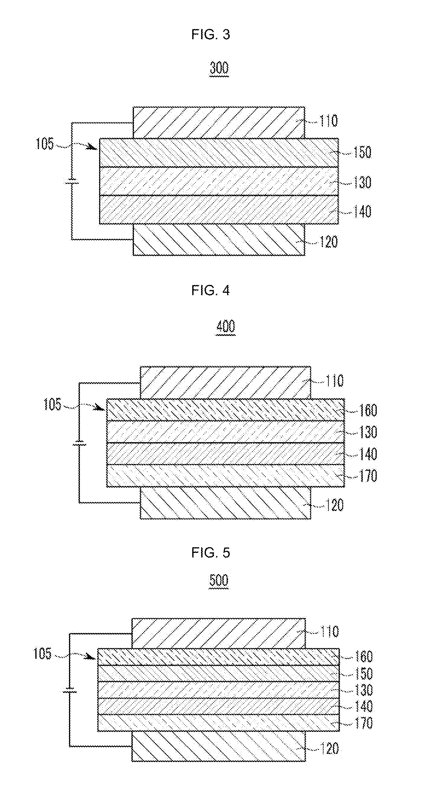
  • Material for organic optoelectronic device, organic light emitting diode including the same, and display including the organic light emitting diode
  • Material for organic optoelectronic device, organic light emitting diode including the same, and display including the organic light emitting diode
  • Material for organic optoelectronic device, organic light emitting diode including the same, and display including the organic light emitting diode

Examples


Example

Example 1

Synthesis of Compound Represented by Chemical Formula H-10

[0209]A compound represented by Chemical Formula H-10 is obtained according to the following method.

[0210]Preparation of Compound A

[0211]62.490 g (0.19 mmol) of 3,6-dibromocarbazole and 11.537 g (0.48 mmol) of sodium hydride dispersed in mineral oil are dissolved in 450 mL of DMF in a 2 L round-bottomed flask in an ice-bath, and the solution is agitated for 40 minutes. Then, another solution prepared by dissolving 61.769 g (0.23 mmol) of 2-chloro-4,6-diphenyl triazine in 450 mL of DMF is slowly added to the agitated solution in a dropwise fashion. The mixture is agitated for 12 hours. The reactant is poured into 2 L of water to complete the reaction, the resulting product is agitated for 30 minutes, and a solid produced therein is filtered. The solid is washed with methanol and then dried. The dried solid is dissolved in 2.4 L of chlorobenzene while being heated, and the solution is agitated at room temperature. Then...

Example

Example 2

Synthesis of Compound Represented by Chemical Formula I-1

[0215]A compound represented by Chemical Formula I-1 is synthesized according to the following method.

[0216]16.622 g (51.59 mmol) of 3-bromo-N-phenylcarbazole, 17.775 g (61.91 mmol) of N-phenylcarbazol-3-yl boronic acid, 200 mL of a mixture of tetrahydrofuran:toluene in a ratio of 1:1, and 100 mL of a 2 M potassium carbonate aqueous solution are mixed in a 500 mL round-bottomed flask having an agitator under a nitrogen atmosphere, and 2.981 g (2.58 mmol) of tetrakistriphenylphosphinepalladium (0) is added thereto. The mixture is heated and refluxed for 12 hours under a nitrogen atmosphere.

[0217]When the reaction is complete, the reactant is poured into methanol, and a solid produced therein is filtered. The solid is sufficiently washed with water and methanol, and then dried. The obtained solid is dissolved in 1 L of chlorobenzene while being heated. The solution is filtered through silica gel, and a solvent remaining...

Example

Example 3

Synthesis of Compound represented by Chemical Formula J-1

[0219]A compound represented by Chemical Formula J-1 is obtained according to the following method.

[0220]Preparation of Compound J-1-1

[0221]204.56 g (815.26 mmol) of 2,5-dibromo-4-methylpyridine, 228.63 g (1875.1 mmol) of boronic acid, 1358 mL of 1,4-dioxane, and 815 mL of a 2 M potassium carbonate aqueous solution are mixed in a 4 L round-bottomed flask having an agitator under a nitrogen atmosphere, and 0 47.1 g (40.76 mmol) of tetrakistriphenylphosphine palladium (0) is added thereto. The mixture is heated and refluxed for 12 hours under a nitrogen atmosphere. When the reaction is complete, an organic layer produced therein is separated, and a solvent therein is completely removed. Then, 120.1 g of a compound J-1-1 (a yield of 60%) was obtained through column chromatography.

[0222]Synthesis of Compound J-1-2

[0223]120.1 g (489.63 mmol) of the compound J-1-1, 58.48 g (195.85 mmol) of iridium chloride, 816 mL of 2-etho...


PUM


Abstract

A material for an organic optoelectronic device including a first compound represented by Chemical Formula A-1 and a second compound represented by Chemical Formula B-1:
wherein, variables R1-R8, Ar1, Ar2, L1, L2, X2, n1, and n2 are described in the specification.

Description

CROSS-REFERENCE TO RELATED APPLICATION[0001]This application claims priority to and the benefit of Korean Patent Application No. 10-2013-0005570 filed on Jan. 17, 2013, and all the benefits accruing therefrom under 35 U.S.C. §119, the content of which is incorporated herein in its entirety by reference.BACKGROUND[0002]1. Field[0003]A material for an organic optoelectronic device, an organic light emitting diode, and a display device including the organic light emitting diode are disclosed.[0004]2. Description of the Related Art[0005]An organic photoelectric device is a device requiring a charge exchange between an electrode and an organic material by using holes or electrons.[0006]An organic optoelectronic device may be classified in accordance with its driving principles. A first organic optoelectronic device is an electronic device driven as follows: excitons are generated in an organic material layer by photons from an external light source, the excitons are separated into electr...

Claims


Application Information

Patent Timeline
IPC IPC(8): H01L51/00
CPCH01L51/0067H01L51/0071H01L51/0074H01L51/0073H01L51/0072C09K11/06C09K2211/185H10K85/615H10K85/654H10K85/657H10K85/6576H10K85/6574H10K85/342H10K85/6572H10K50/11H10K2101/90H10K85/631H10K50/12
Inventor KIM, HYUNG-SUNKIM, BYUNGKUKIM, CHANG WOORYU, JIN HYEONPARK, MOO-JINYANG, JAE-DEUKYU, EUN-SUNLEE, HO-JAE
Owner SAMSUNG ELECTRONICS CO LTD
Why Eureka
Try Eureka