DRAM Memory Interface

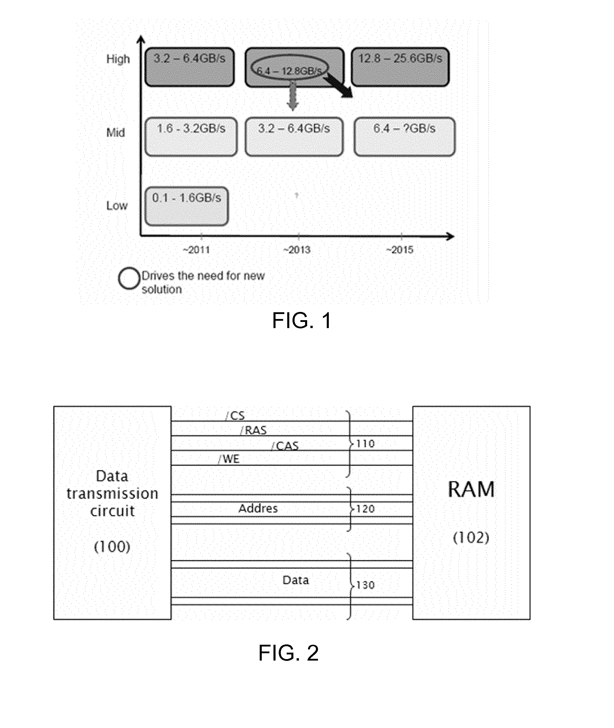
a memory interface and dram technology, applied in the field of dram (dynamic random access) memory, can solve the problems of increasing the complexity of software applications, the difficulty of double the highest defined bandwidth today, and the need for ram modules with both larger capacities and higher speeds, so as to reduce the energy consumption of dram interfaces and increase the bandwidth of dram interfaces

Inactive Publication Date: 2014-07-17
ST ERICSSON SA
View PDF2 Cites 0 Cited by
  • Summary
  • Abstract
  • Description
  • Claims
  • Application Information

AI Technical Summary

Benefits of technology

[0012]An object of embodiments of the present invention is to alleviate at least partly the above mentioned drawbacks. More particularly, embodiments of the invention aim at improving the way of reducing the energy

Problems solved by technology

As software applications become more complex and work with larger amounts of data, RAM modules having both larger capacities and higher speeds are needed.
However, it becomes difficult to double the highest defined bandwidth today with a full swing signal and not terminated path.
Indeed, the increase of the bandwidth is in general performed by increasing the frequency at which the signals are transmitted, which consequently involves integrity problems for the transmitted signals.
Consequently, signal integrity constrains the physical (PHY) layer, and therefore the package, and as a result, the development and material cost is increased.
Furthermore, the increase of the bandwidth is also accompanied with an increase of the power consumption.
Indeed, power consumption (and heat to be dissipated) increases with the speed, e.g.

Method used


Image

  • DRAM Memory Interface
  • DRAM Memory Interface
  • DRAM Memory Interface

Examples


Embodiment Construction

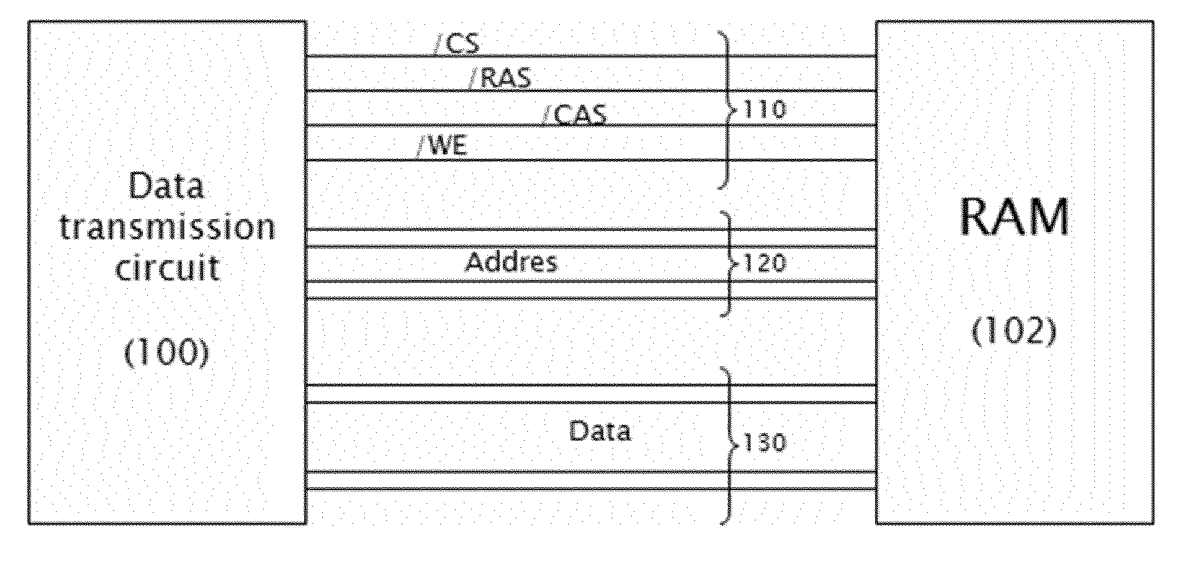
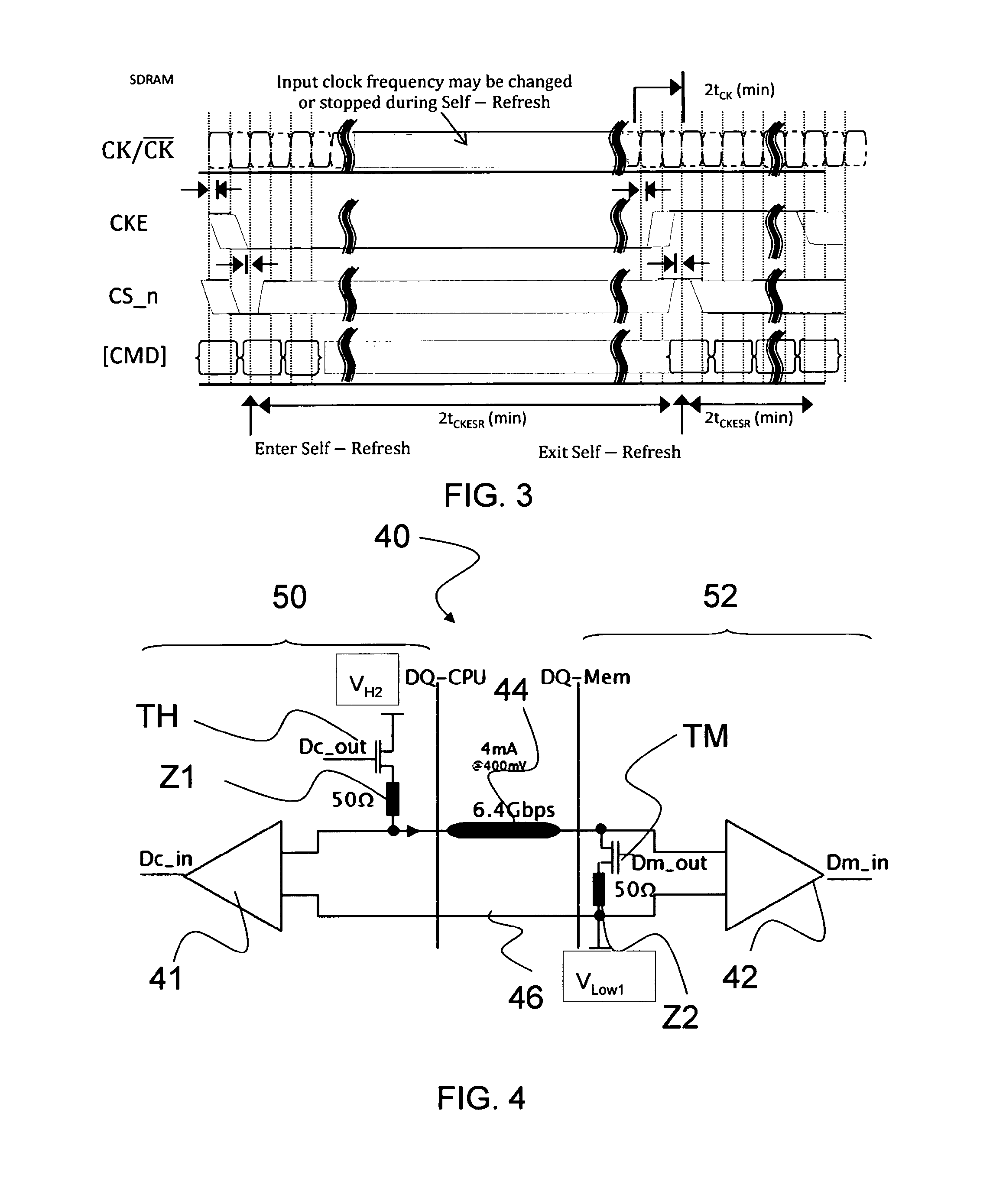
[0056]Referring to FIG. 5, it is shown an illustration of a schematic circuit block diagram showing data transmission between a CPU / host side and a memory. Especially, FIG. 5 shows an example of a DRAM memory interface 54 for transmitting signals between a memory controller device 50 and a DRAM memory device 52. The term memory interface refers to the means for allowing interactions between components and how these interactions are performed. A DRAM memory interface is thus hardware that allows a memory controller device and a DRAM memory device to communicate; the DRAM memory interface works as an input / output system between the memory and its controller.

[0057]The CPU / host, or memory controller device, may be, but not limited to, a piece of hardware dedicated to the management of the memory. The memory controller device may be also a CPU (Computer Processing Unit), or at least managed by the CPU. The memory controller device may also be a computer program executable by hardware (e....


PUM


Abstract

It is proposed a DRAM memory interface (40) for transmitting signals between a memory controller device (50) and a DRAM memory device (52). The DRAM memory interface comprises: data lines (44) for transmitting data signals; one or more control line(s) for transmitting control signals; one or more address line(s) for transmitting address signals; for each line, a transmitter device (41) connected to a first end of the line and a receiver device (42) connected to a second end of the line; wherein: each line is a single ended line wherein a signal transmitted on the line is referenced to a first reference voltage line (46); and —each line has an termination (Z1, Z2) on both the first and second ends of the line by connecting a first impedance (Z1) to the first end of the line and a second impedance (Z2) to the second end of the line.

Description

TECHNICAL FIELD[0001]The invention relates to the field of DRAM (Dynamic random-access) memory, especially to DRAM interfaces for transmitting data between a CPU / Host / Core and a DRAM memory device.BACKGROUND ART[0002]Up to now the Dynamic Random Memory (DRAM) interface uses a parallel link, as defined in several JDEC standards, e.g. JEDEC (Joint Electron Device Engineering Council) DDR1 / DDR2 / DDR3, JEDEC LPDDR1 / LPDDR2, JEDEC GDDR3 / GDDR4 / GDDR5.[0003]Memory interface (also referred to as memory bus) requires more and more bandwidth between a host (e.g. a processor) and the memory device. Indeed, as discussed in the United States Patent Application 2006 / 0136658, random access memory (RAM) plays a critical role in the operation of computing systems. The performance of computing systems and the software applications executed thereon depends on both the capacity and the speed of the RAM modules used. As software applications become more complex and work with larger amounts of data, RAM mod...

Claims


Application Information

Patent Timeline
IPC IPC(8): G11C11/406G11C11/402
CPCG11C11/4023G11C11/40615G11C5/063G11C7/02G11C7/1048G11C7/1057G11C7/1084G11C11/4093
Inventor BERTHOLOM, CEDRIC
Owner ST ERICSSON SA
Why Eureka
Try Eureka