Method for fabricating mesa sidewall with spin coated dielectric material and semiconductor element thereof

a dielectric material and spin coating technology, applied in the field of semiconductor technology, can solve the problems of increasing the leakage current of the element, affecting and the defect rate of the element is very high, so as to enhance the mechanical strength of the element

Inactive Publication Date: 2014-08-07
NAT CENT UNIV
View PDF5 Cites 0 Cited by
  • Summary
  • Abstract
  • Description
  • Claims
  • Application Information

AI Technical Summary

Benefits of technology

[0008]The first objective of the present invention is to provide a method for fabricating a mesa sidewall with a spin coated dielectric material, thereby enhancing the mechanical strength of the element.
[0009]Another objective of the present invention is to provide a method for fabricating a mesa sidewall with a spin coated dielectric material so as to prevent the element from collapsing.
[0010]Another objective of the present invention is to provide a semiconductor element fabricated by said method to enhance its physical strength.
[0023]The spirit of the present invention is to coat the semiconductor sample with the liquid dielectric material, to expose the upper metal object (or the structure unaffected by ion bombardment) of the semiconductor element by an etching process so as to form an insulation oxidation sidewall or an extended protrusion (SiO2 or SiNx), and further to use the sidewall or the extended protrusion as an etching mask to anisotropically etch and remove the exposed liquid dielectric material so that a mesa sidewall made from the liquid dielectric material is formed. This process can substitute the deposition process in the conventional art to avoid unnecessary damage to the element. Beside, the process also enhances the mechanical strength thereof.

Problems solved by technology

However, such elements have a very high defect rate due to the fabrication process.
Among them, PECVD has a good coating effect but ion bombardment would occur when the sidewall grows, which in turn increases leakage current in the element.
ICP-CVD has a poor ability to fill up gaps and tends to form holes.
ALD has a good ability to fill up gaps and a good surface coating effect; its drawback is slow growth, which slows down the overall fabrication speed.

Method used


Image

  • Method for fabricating mesa sidewall with spin coated dielectric material and semiconductor element thereof
  • Method for fabricating mesa sidewall with spin coated dielectric material and semiconductor element thereof
  • Method for fabricating mesa sidewall with spin coated dielectric material and semiconductor element thereof

Examples


first embodiment

The First Embodiment

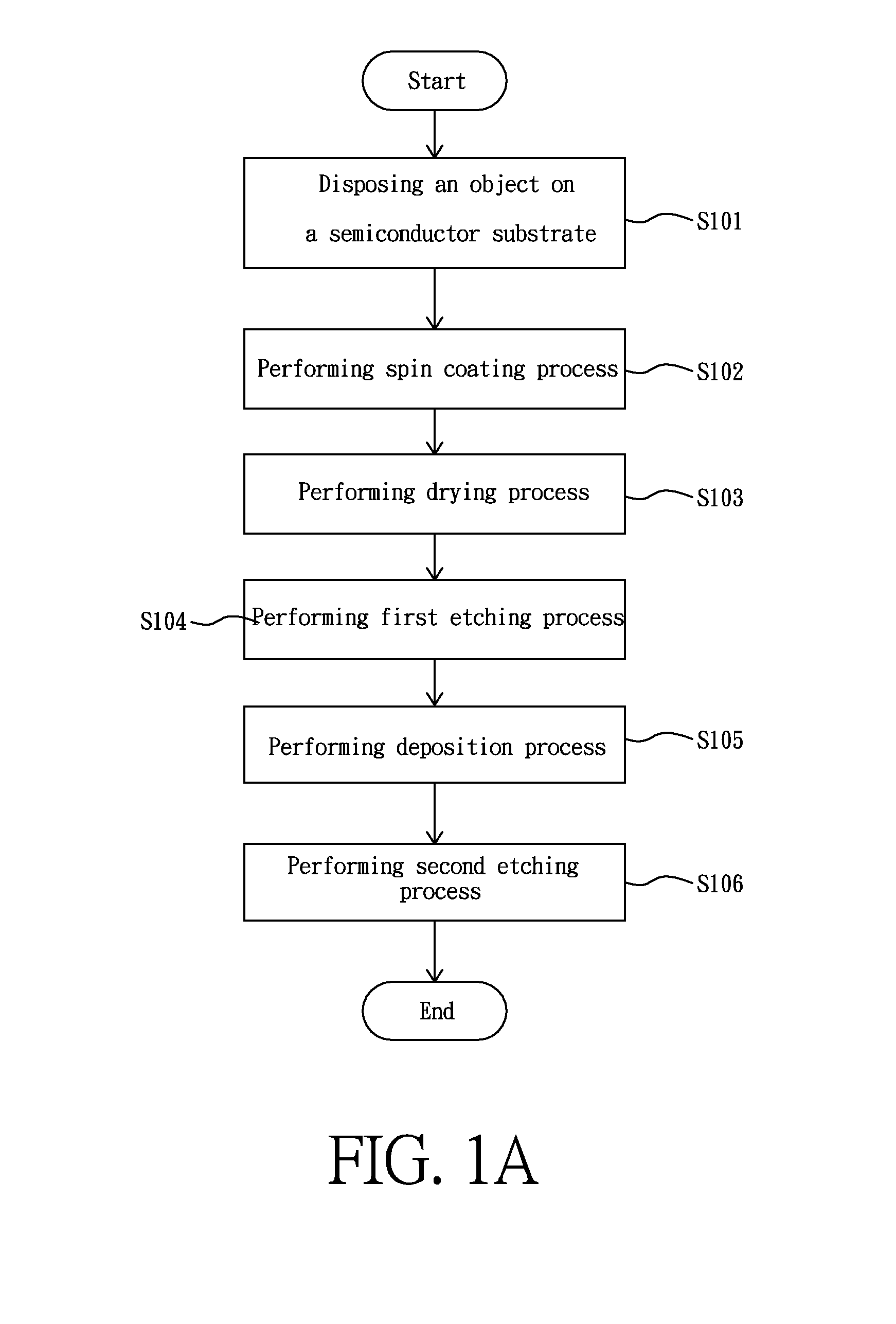
[0057]FIG. 1A is a flow chart depicting a method for fabricating a mesa sidewall with a spin coated dielectric material according to the first embodiment of the present invention. As seen in FIG. 1A, said method for fabricating a mesa sidewall with a spin coated dielectric material includes the following steps:

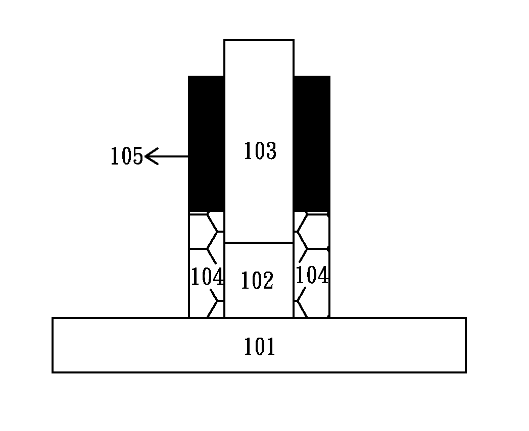
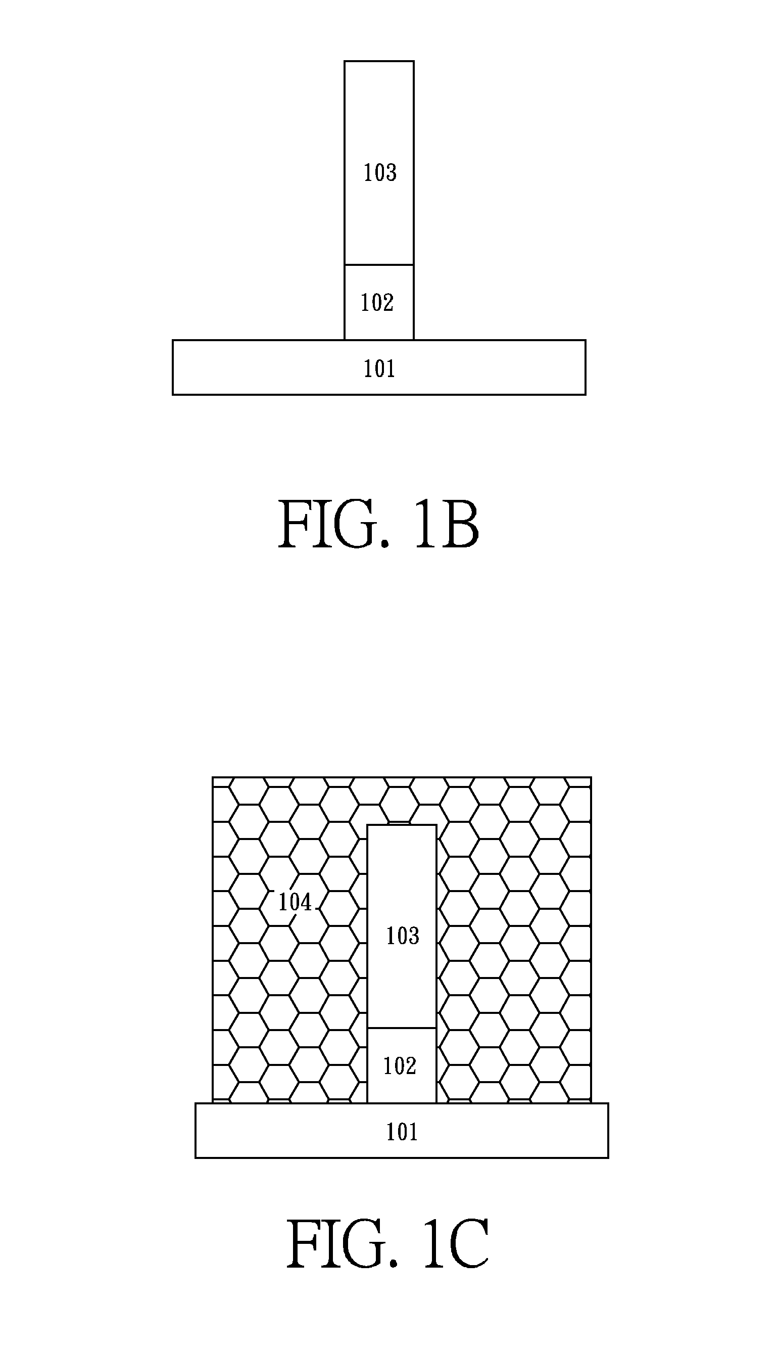
[0058]Step S101: Disposing an object on a semiconductor substrate. FIG. 1B shows a schematic drawing of Step S101 in the method for fabricating a mesa sidewall with a spin coated dielectric material according to the first embodiment of the present invention. As seen in FIG. 1B, 101 is a semiconductor substrate; 102 is a mesa structure to be coated with a liquid dielectric material; 103 is a structure unaffected by ion bombardment, and generally 103 may be a metal, a high doped semiconductor or a dielectric material. For the convenience of explanation, a metal is used as an example. Generally, 102, the mesa structure to be coated with a liquid dielectric mat...

second embodiment

The Second Embodiment

[0065]FIG. 2A is a flow chart depicting a method for fabricating a mesa sidewall with a spin coated dielectric material according to the second embodiment of the present invention. FIG. 2B is a schematic drawing of Step S201 in the method according to the second embodiment of the present invention. As seen in FIG. 2B, in this embodiment, the element has a wide-top-narrow-bottom structure similar to the English alphabet “T.” Fabrication processes vary with different shapes.

[0066]Next, reverting back to FIG. 2A, the method for fabricating a mesa sidewall with a spin coated dielectric material includes the following steps:

[0067]Step S201: Forming a wide-top-narrow-bottom T-shape element over a semiconductor 201, as seen in 203 and 202 of FIG. 2B.

[0068]Step S203: Performing a spin coating process to coat with a liquid dielectric material. FIG. 2C is a schematic drawing of Step S203 in the method for fabricating a mesa sidewall with a spin coated dielectric material ...

third embodiment

The Third Embodiment

[0072]FIG. 3A is a flow chart depicting a method for fabricating a mesa sidewall with a spin coated dielectric material according to the third embodiment of the present invention. FIG. 3B is a schematic drawing of Step S301 in the method according to the third embodiment of the present invention. As seen in FIG. 3B, in the third embodiment, the structure of the element has a metal 303 (or a structure unaffected by ion bombardment) disposed over a semiconductor 302, and semiconductor 302 disposed over a semiconductor substrate 301. Unlike the third embodiment, the metal of the second embodiment has a wide-top-narrow-bottom shape similar to the English alphabet “T,” while in the third embodiment a wet etching process is performed to form an undercut structure at gaps filled with the dielectric material.

[0073]Next, reverting back to FIG. 3A, the method for fabricating a mesa sidewall with a spin coated dielectric material has the following steps:

[0074]Step S301: Fir...


PUM

PropertyMeasurementUnit
operating frequencyaaaaaaaaaa
dielectricaaaaaaaaaa
widthaaaaaaaaaa

Abstract

A method for fabricating a mesa sidewall with a spin coated dielectric material and a semiconductor element fabricated by the same are provided in the present invention. The method includes the steps of: disposing an object on a semiconductor substrate; performing a spin coating process to coat with a liquid dielectric material; performing a drying process to dry the liquid dielectric material; performing a first etching process to remove an upper part of the dried dielectric material to expose a metal part (unaffected by ion bombardment) of the object; performing a deposition process to insulate the metal part (unaffected by ion bombardment) of the object; and performing a second etching process to form a semiconductor element with a mesa sidewall.

Description

[0001]This application claims the benefit of TW Application No. 102104500 filed on Feb. 2, 2013, the content of which is hereby incorporated by reference.BACKGROUND OF THE INVENTION[0002]1. Field of Invention[0003]The present invention relates in general to the technology of fabricating semiconductors, and more particularly to a method for fabricating a mesa sidewall with a spin coated dielectric material.[0004]2. Related Art[0005]High-speed III-V electronic devices have played a key role in broadband communication. They are extensively used in wireless communication equipment, and have proved to be indispensable in the 40 Gb / s optical fiber communication system as well. Recent years witness the ever-growing demand for larger broadband width and higher speed as technology advances. People have started to pay attention to circuits with an operating frequency higher than 300 GHz and the realization of terahertz transistors, as seen applied in wireless communication, security maintenan...

Claims


Application Information

Patent Timeline
Patent Type & Authority Applications(United States)
IPC IPC(8): H01L21/02H01L29/737H01L29/778
CPCH01L21/02282H01L29/778H01L29/737H01L21/31144H01L29/41708H01L29/42316H01L29/7371
Inventor CHYI, JEN-INNWANG, SHENG-YUCHEN, JIUN-MING
Owner NAT CENT UNIV
Why Eureka
Try Eureka