
MEMS Force Sensors Fabricated Using Paper Substrates

a technology of paper substrates and force sensors, applied in the field of two and three dimensional paper sensors, can solve the problems of limiting the potential use of mems devices in many applications, requiring costly materials, and being conducted in a cleanroom environmen

Inactive Publication Date: 2014-08-14
PRESIDENT & FELLOWS OF HARVARD COLLEGE
View PDF4 Cites 36 Cited by
  • Summary
  • Abstract
  • Description
  • Claims
  • Application Information

AI Technical Summary

Benefits of technology

The present invention is about creating sensors using paper and other inexpensive materials like fabric or plastic film. These sensors can be made in two dimensions or three dimensions. The shape and chemical properties of the paper can be used to create the sensor's structure and function. Overall, this invention provides a cost-effective and easy way to create durable and flexible sensors.

Problems solved by technology

While these fabrication strategies can produce silicon-based MEMS which exhibit excellent device performance, they are typically time consuming, require costly materials, and must be conducted in a cleanroom environment.
As a result, MEMS devices are relatively costly, limiting their potential use in many applications.

Method used


Image

  • MEMS Force Sensors Fabricated Using Paper Substrates
  • MEMS Force Sensors Fabricated Using Paper Substrates
  • MEMS Force Sensors Fabricated Using Paper Substrates

Examples


example 1

Fabrication of a Paper-Based Piezoresistive Force Sensor

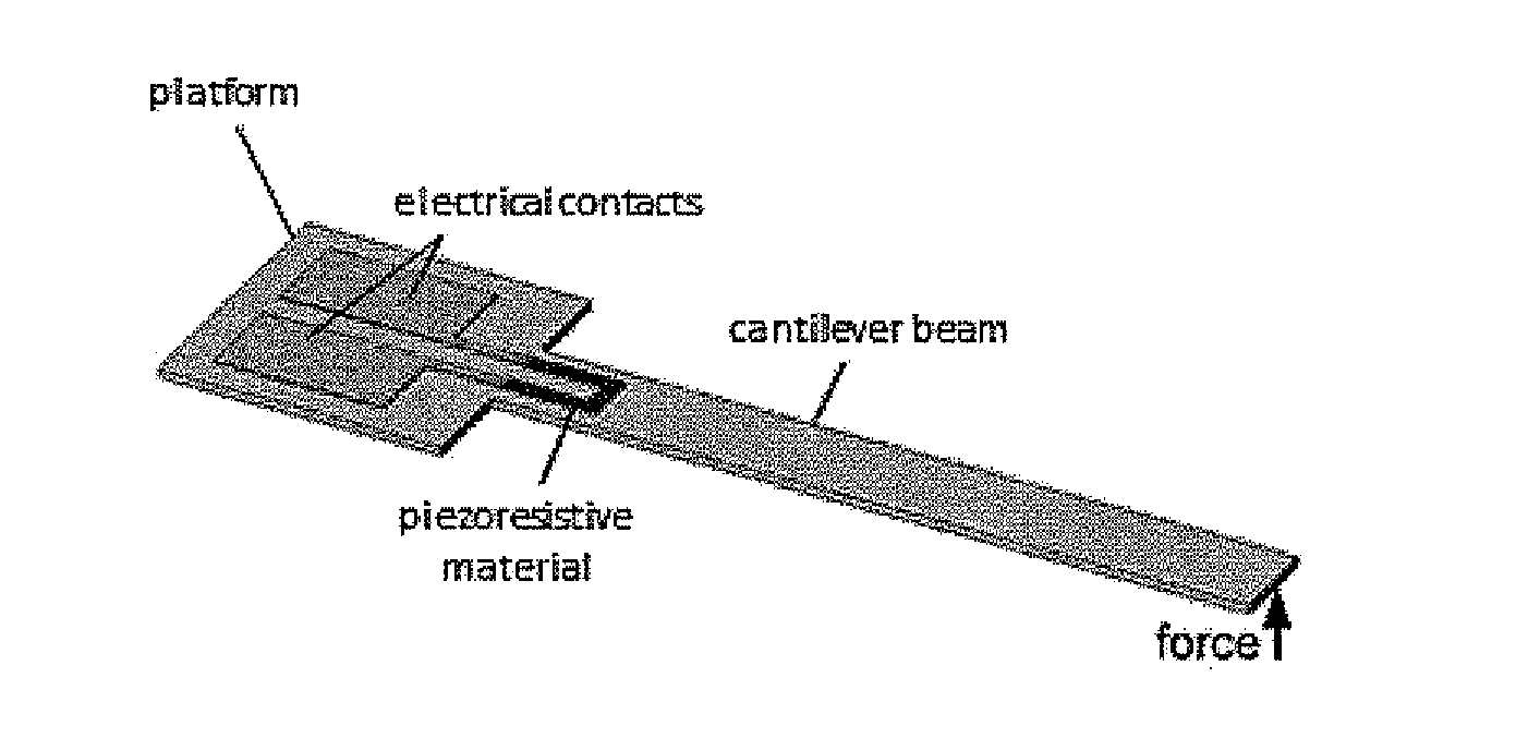
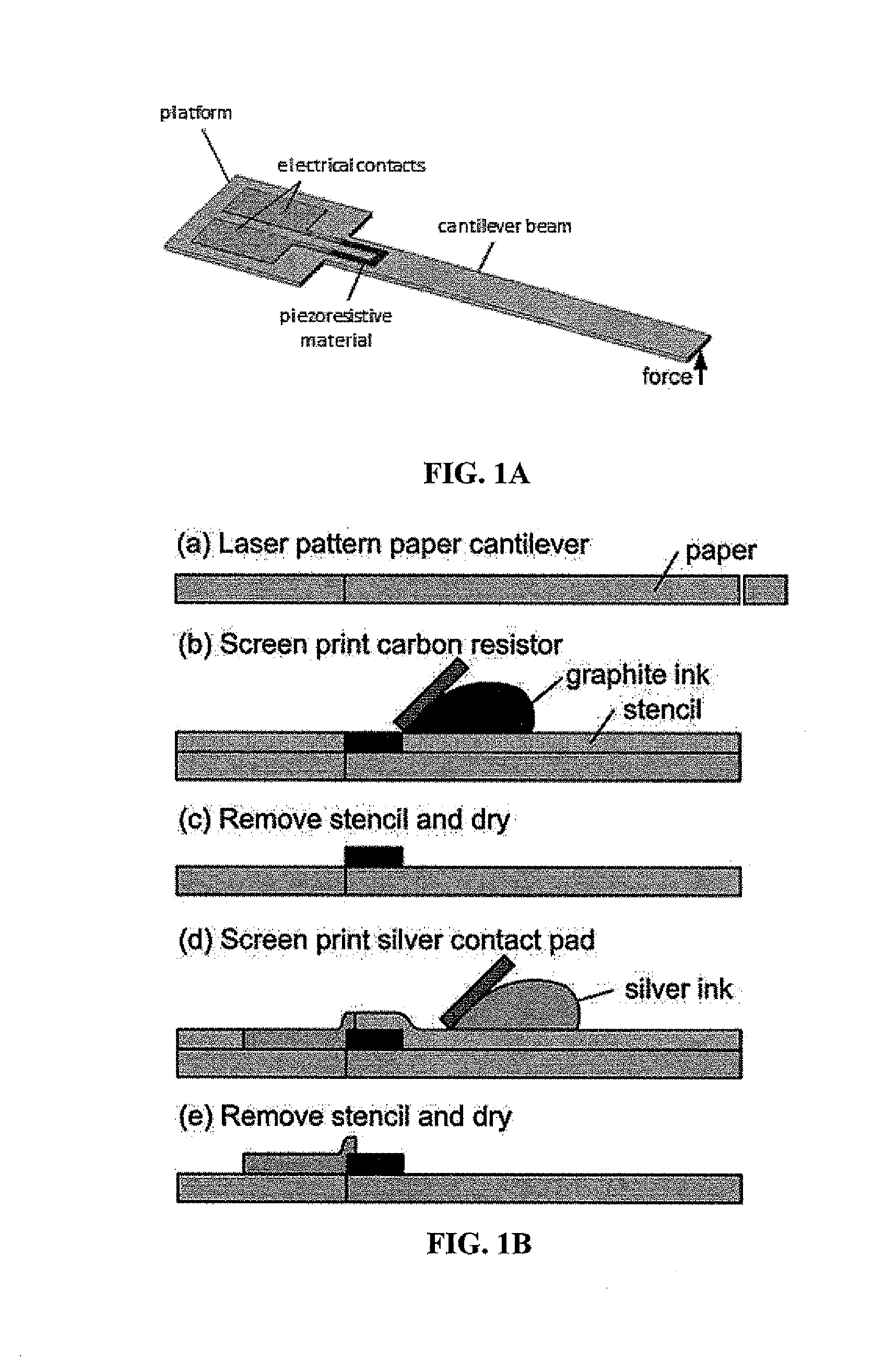
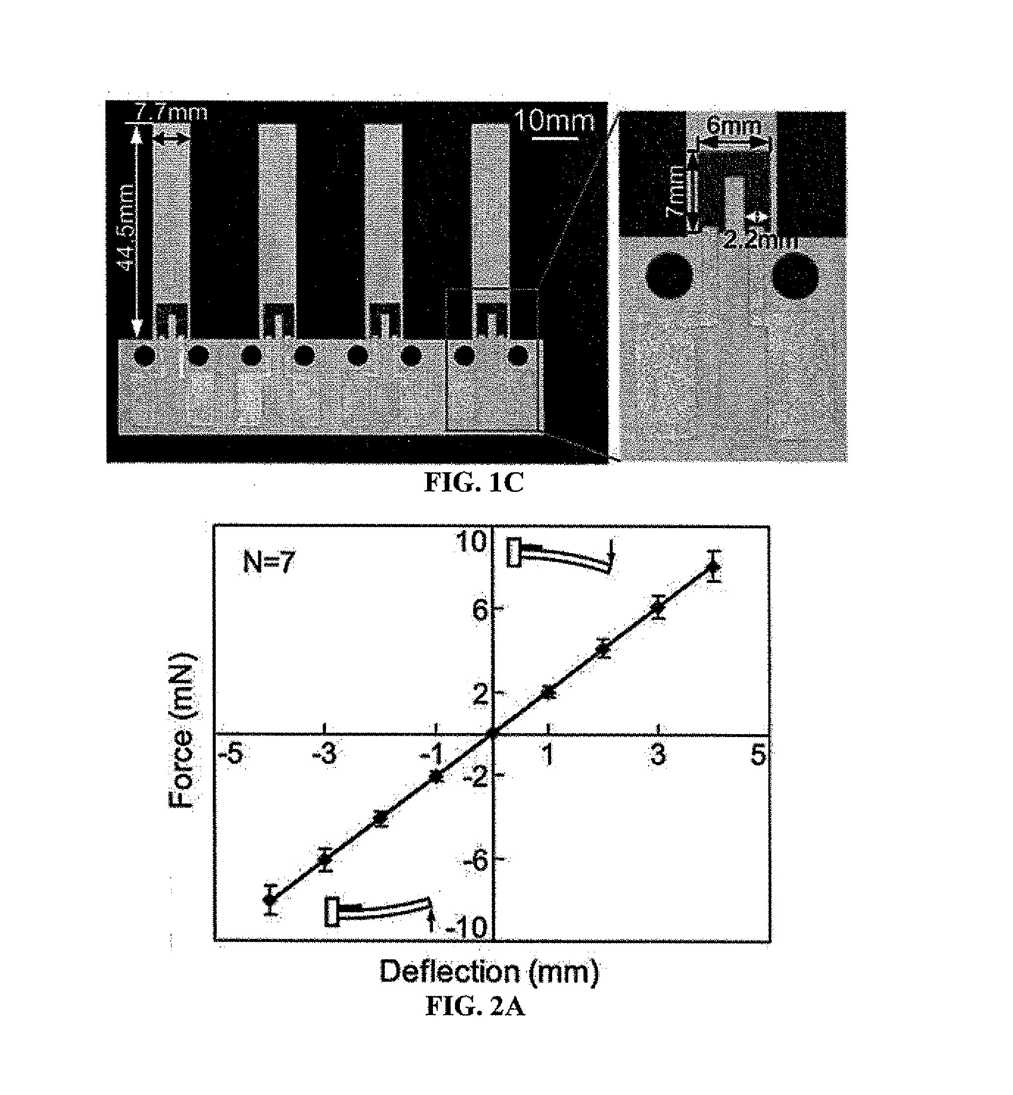
[0148]FIG. 1A shows a schematic diagram of a simple, paper-based force-sensing cantilever. In this device, a carbon resistor is located at the root of the cantilever, where the maximum surface strain occurs during detection. The carbon resistor was designed to be short (7 mm) relative to the length (44.5 mm) of the cantilever. When a force is applied to the beam structure, the resistor experiences a mechanical strain / stress, which then induces a change in resistance of the resistor. Measuring the change in resistance allows quantification of the applied force.

[0149]The fabrication of the cantilever beam force sensor is illustrated in FIG. 1B. Whatman® 3MM chromatography paper (catalog number: 3030-6185, 340 μm thick, 186 g / m−2) was selected as a paper substrate for purposes of initial investigation. To render the paper hydrophobic, the surface hydroxyl groups of the paper were functionalized (cellulose fibers) with (tridecafluo...

example 2

Smart Paper Cube: a Three-Axis MEMS Accelerometer

[0179]Paper was used as the structural material for constructing a three-axis MEMS accelerometer. The device measures accelerations based on the principle of piezoresistive effect generated by conductive materials patterned on a paper structure. Three one-axis piezoresistive sensing elements and their readout circuits are first laid out on a piece of patterned paper, and the paper is then folded to form a cube (which we call “smart paper cube”). The three sensing elements are configured on the paper substrate in such a fashion that they locate on three orthogonal surfaces of the paper cube after folding.

[0180]FIGS. 8A-C show a paper-based weighing balance. FIG. 8A shows a schematic side view of a paper-based balance where force-sensing beams with carbon resistors are used for tethering a weighing plate, and measuring the force due to gravity of a weight. FIG. 88 shows the paper-based balance where four force sensing beams are involved...

example 3

Paper as a Hydrophobic Surface

[0188]A hydrophobic surface on paper (i.e., cellulose) was created. A hydrophobic surface is formed on paper by silanizing the surface of paper (cellulose) fibers through chemical vapor deposition. By using different types of chemical reactions to introduce fluorinated and non-fluorinated groups, it was demonstrated that the observed hydrophobicity is due to the exposed surface groups and not the capping of hydroxyl groups on the surface. The linkage bonds were exploited to form pH-sensitive hydrophobic paper surfaces.

[0189]Procedure and Result

[0190]Hydrophobic Paper

[0191]To render paper hydrophobic, the hydroxyl groups of the paper cellulose fibers were functionalized with (tridecafluoro-1,1,2,2-tetrahydrooctyl)trichlorosilane vapor to form surface silanol linkages, and thus generated a hydrophobic surface (FIG. 16A). Six types of paper were silanized and measured for their water contact angles (FIG. 16B) using a contact angle goniometer. Among these t...


PUM


Abstract

MEMS devices fabricated using inexpensive substrate materials such as paper or fabric, are provided. Using paper as a substrate, low cost, simple to prepare, lightweight, disposable piezoresistive sensors, including accelerometers are prepared. Signal-processing circuitry can also be patterned on the substrate material.The sensors can be utilized as two-dimensional sensors, or the paper substrate material can be folded to arrange the sensors in a three dimensional conformation. For example, three sensors can be patterned on a paper substrate and folded into a cube such that the three sensors are orthogonally positioned on the faces of a cube, permitting simultaneous measurement of accelerations along three orthogonal directions (x-y-z). These paper-based sensors can be mass produced by incorporating highly developed technologies for automatic paper cutting, folding, and screen-printing.Also provided are methods of modifying paper for use as a substrate material in MEMS devices.

Description

CROSS-REFERENCE TO RELATED APPLICATIONS[0001]This application claims priority under 35 U.S.C. §119 to U.S. Provisional Application Ser. No. 61 / 513,977 filed Aug. 1, 2011.STATEMENT REGARDING FEDERALLY SPONSORED RESEARCH OR DEVELOPMENT[0002]This invention was made with Government Support under N66001-10-1-4003 awarded by the U.S. Department of the Navy. The Government has certain rights in the invention.FIELD OF THE INVENTION[0003]The present invention relates to two and three dimensional paper sensors which are high economical and easy to manufacture and use.BACKGROUND OF THE INVENTION[0004]Improved methods of microfabrication have permitted the construction of micro-electro-mechanical systems (MEMS) for use in a wide array of important applications. Commercial applications include digital micromirror devices (DMD; Texas Instruments), accelerometers used in consumer electronics and automobiles (e.g., to detect collisions and trigger airbag deployment; Analog Devices and Motorola), gy...

Claims


Application Information

Patent Timeline
IPC IPC(8): G01P15/12B81B7/02
CPCB81B7/02G01P15/123G01P15/0802G01P15/18G01L1/18G01P2015/0862B81C1/0015G01G3/13
Inventor WHITESIDES, GEORGELIU, XINYULI, XIUJUNTHUO, MARTIN M.O'BRIEN, MICHAELSUN, YU
Owner PRESIDENT & FELLOWS OF HARVARD COLLEGE
Learn More