Method for Producing Structured Sintered Connection Layers, and Semiconductor Element Having a Structured Sintered Connection Layer

a technology of structured sintered layers and semiconductor elements, which is applied in the direction of basic electric elements, manufacturing tools, solid-state devices, etc., can solve the problems of adverse effect on the stability and reliability of the sinter layer, and achieve the effect of satisfying the electrical and thermal connection, reducing mechanical tension within the chip, and increasing surface coverag

Active Publication Date: 2014-08-14
ROBERT BOSCH GMBH
View PDF5 Cites 5 Cited by
  • Summary
  • Abstract
  • Description
  • Claims
  • Application Information

AI Technical Summary

Benefits of technology

[0008]One basic aspect of the present invention is the production of a sinter layer connection between a substrate and a chip which produces a satisfactory electric and thermal connection between the substrate and the chip and also reduces mechanical tensions within the chip. This is achieved by a sinter layer made up of a multitude of sinter elements, which are placed in structured manner between the substrate and chip produced from a contact area. Because of a higher surface coverage density of the sinter elements in the center of the contact area it is possible to ensure excellent thermal and electrical conductivity in the particular locations where high temperatures typically develop when the chip is in operation. The surface coverage density of the sinter elements at the edge of the contact area is lower than in the center, so that the compression pressure there on each sinter element during the sintering process is effectively higher than in the center, which enhances the reliability of the sinter connection in the edge region.
[0009]A through channel to each sinter element is formed along the main surface of the substrate between chip and substrate, so that gassing and degassing is ensured for all sinter elements during the sintering process. In particular the oxygen supply, which is required for adequate sintering, is able to be ensured via the through channels for each sinter element. At the same time, the gases emitted by the sinter elements during the sintering process are able to be discharged via the through channels, so that a uniform and predictable development of the sinter layer in all regions of the contact area is advantageously possible.
[0010]In an advantageous manner, many sinter elements are able to be formed in the edge region, in particular, so that the entire thermal or electrical conductivity of the sinter layer will not be adversely affected even if individual sinter connections fail during or after the sintering operation, i.e., if there is a lack in thermal or electrical conductivity across individual sinter elements, because other sinter elements in the edge region are able to assume the function of the malfunctioning sinter elements.
[0011]It may be advantageous to gradually increase the surface coverage density of the sinter elements on the substrate in a region of the contact area between the center region and edge region, from the surface coverage density in the edge region toward the surface coverage density in the center region of the contact area.
[0012]The edge of the contact area in the lateral direction along the main surface of the substrate may advantageously be set apart from the edges of the chip by a predefined length. This may advantageously reduce mechanical stressing of the fracture-prone chip edge.
[0013]In addition, it may be advantageous to select a larger lateral extension of the sinter elements in the center region of the contact area, in comparison with the lateral extension of the sinter elements in the edge region of the contact area. For one, this achieves a high surface coverage density in the mechanically less stressed center region of the contact area, which therefore results in improved thermal and electrical contacting of the sinter layer with the chip. For another, because of the lower surface coverage density in the edge region, the effective sinter pressure on each of the smaller sinter elements is increased in the edge region, which means that there is greater reliability of the sintering process and of the stability of the sinter connection in the mechanically heavily stressed edge region of the contact area.

Problems solved by technology

Because of the different coefficients of thermal expansion of semiconductors and metallic layers, mechanical warping may occur in the sinter layer, which could have an adverse effect on the stability and reliability of the sinter layer.

Method used


Image

  • Method for Producing Structured Sintered Connection Layers, and Semiconductor Element Having a Structured Sintered Connection Layer
  • Method for Producing Structured Sintered Connection Layers, and Semiconductor Element Having a Structured Sintered Connection Layer
  • Method for Producing Structured Sintered Connection Layers, and Semiconductor Element Having a Structured Sintered Connection Layer

Examples


Embodiment Construction

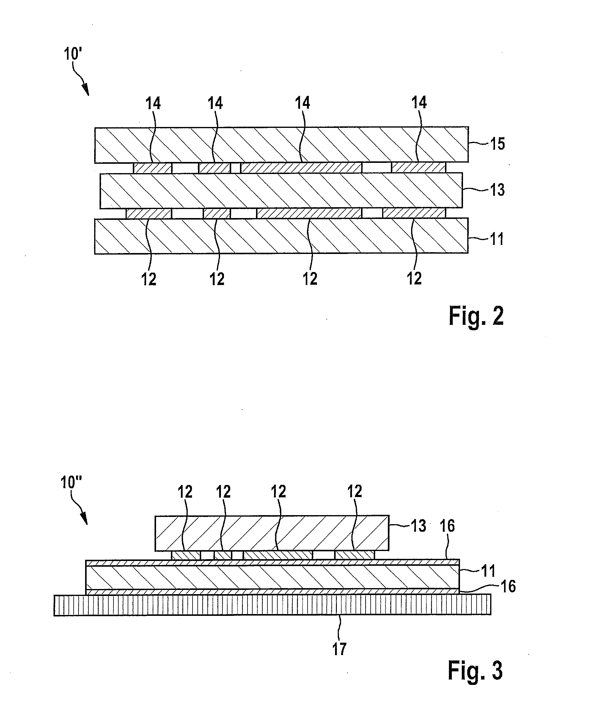
[0022]Unless stated otherwise, identical or functionally equivalent elements, features and components have been provided with the same reference symbols. It is understood that components and elements in the figures are not necessarily depicted true to scale with respect to one another for reasons of clarity and comprehensibility.

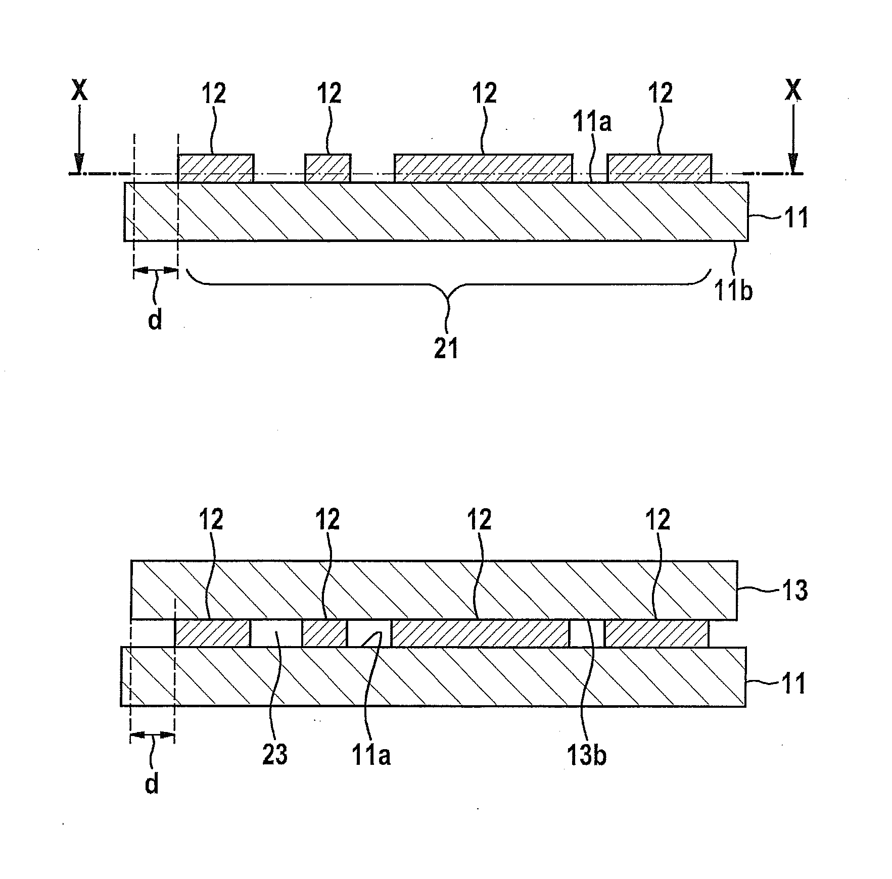
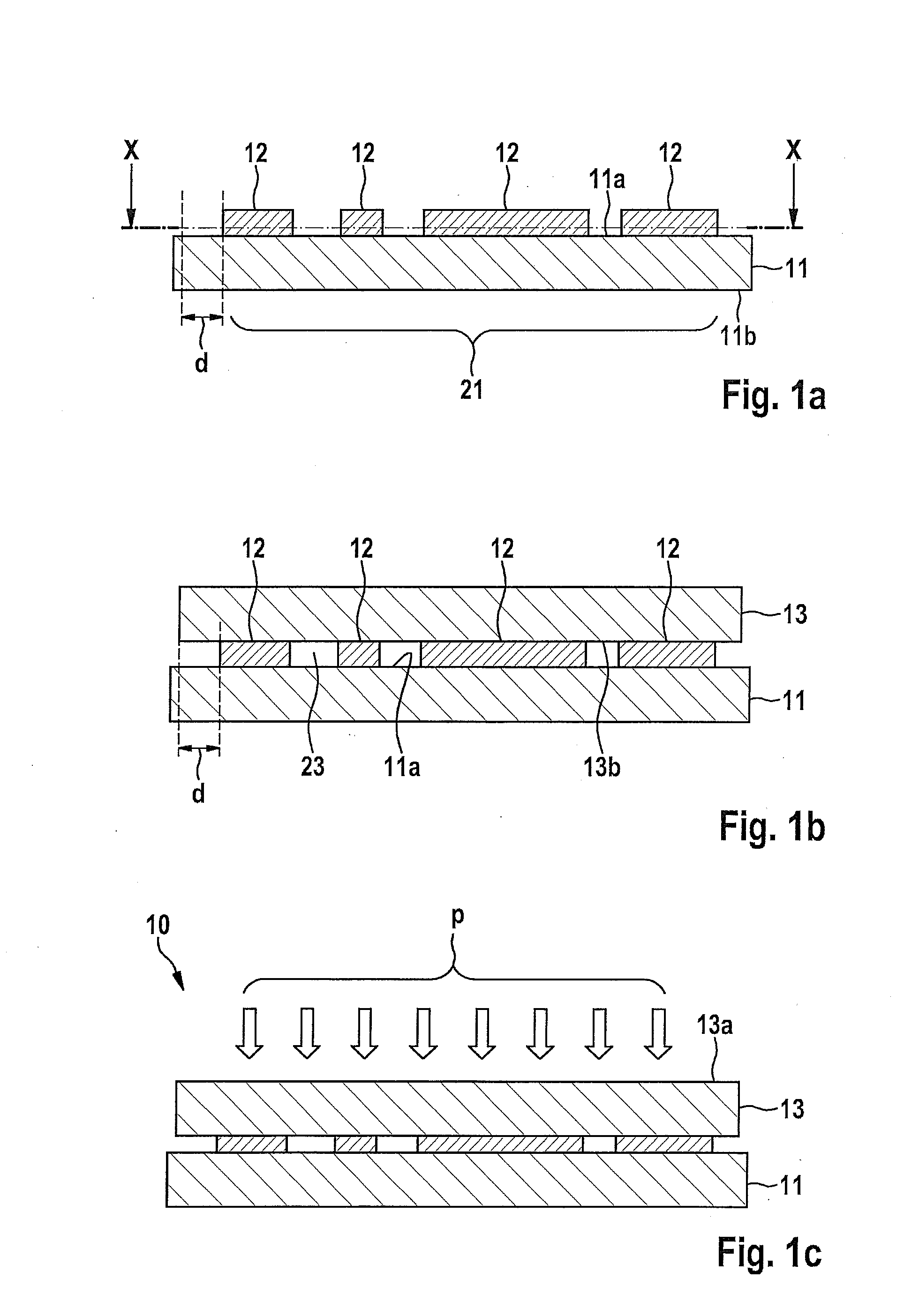
[0023]FIGS. 1a through 1c show stages of a method for producing structured sinter layers 12 on a substrate 11. FIG. 1a shows a schematic representation of a substrate 11 having a first main surface 11a and a main surface 11b which lies opposite first main surface 11a. For example, substrate 11 may be a metal substrate, especially a copper substrate, or a substrate coated with metal. A noble metal surface, e.g., because of a nickel-gold metal coating on a copper substrate, is able to ensure excellent adhesion of the sinter layer on the substrate. Sinter elements for the development of a sinter layer 12 may be applied on main surface 11a. For example, the sint...


PUM

PropertyMeasurementUnit
thicknessaaaaaaaaaa
thicknessaaaaaaaaaa
thicknessaaaaaaaaaa

Abstract

A method for producing a sinter layer connection between a substrate and a chip resulting in an electric and thermal connection therebetween and in reduced mechanical tensions within the chip. The method produces a sinter layer by applying a multitude of sinter elements of a base material forming the sinter layer in structured manner on a contact area of a main surface of a substrate; placing a chip to be joined to the substrate on the sinter elements; and heating and compressing the sinter elements to produce a structured sinter layer connecting the substrate and chip and extending within the contact area, the surface coverage density of the sinter elements on the substrate in a center region of the contact area being greater than the surface coverage density of the sinter elements in an edge region of the contact area, and at least one through channel, extending laterally as to the substrate's main surface being provided towards the contact area's edge. A large-area sinter element is situated in the contact area's center region, and circular sinter elements is situated in a contact area edge region. The sinter elements may also have notches. Also described is a related device.

Description

FIELD OF THE INVENTION[0001]The present invention relates to a method for producing structured sintered layers and to a semiconductor component, especially a power electronics component, having a structured sintered layer.BACKGROUND INFORMATION[0002]Electronic components such as power diodes, (vertical) power transistors or other components must be mounted on substrates. Because of the high currents through such components, it is important to ensure excellent electric and thermal coupling between the components and the substrate.[0003]It is possible to use sintered connections on silver basis (silver sintering) for the mechanical connection between semiconductors and metallic layers, e.g., copper layers, such as the Low-Temperature Connection Technology of Power Electronics (Fortschritt Reports of the VDI, series 21, No. 365, VDI-Verlag), and related methods. In silver sintering, a paste including micro particles or nano particles is compressed under increased temperature and increa...

Claims


Application Information

Patent Timeline
Patent Type & Authority Applications(United States)
IPC IPC(8): H01L23/00
CPCH01L23/3735H01L24/27H01L24/29H01L24/30H01L24/32H01L24/83H01L2224/2732H01L2224/27418H01L2224/27848H01L2224/29012H01L2224/29015H01L2224/29023H01L2224/29139H01L2224/3003H01L2224/30051H01L2224/3012H01L2224/30142H01L2224/3016H01L2224/30181H01L2224/83048H01L2224/83203H01L2224/8384H01L2924/01047H01L2924/1301H01L2924/1305H01L2924/13055H01L2924/13062H01L2924/13091H01L2924/1517H01L2924/15747H01L2924/3512H01L2224/29H01L2224/29298H01L2924/01005H01L2924/00011H01L2924/01029H01L2924/00013H01L2224/29099H01L2224/29199H01L2224/29299H01L2224/2929H01L2924/07811H01L24/64H01L24/70H01L2924/15787H01L2224/29007H01L2224/32014H01L2224/29036H01L2224/73103H01L2224/73203H01L2924/00H01L2924/00012
Inventor GUYENOT, MICHAELGUENTHER, MICHAELHERBOTH, THOMAS
Owner ROBERT BOSCH GMBH
Why Eureka
Try Eureka