

Semiconductor Device
a technology of semiconductors and semiconductors, applied in the field of semiconductor devices, can solve the problems of reducing operation characteristics and increasing manufacturing costs, and achieve the effects of suppressing the increase in the chip area, improving reliability, and low power consumption
- Summary
- Abstract
- Description
- Claims
- Application Information
AI Technical Summary
Benefits of technology
Problems solved by technology
Method used
Image

Examples
embodiment 1
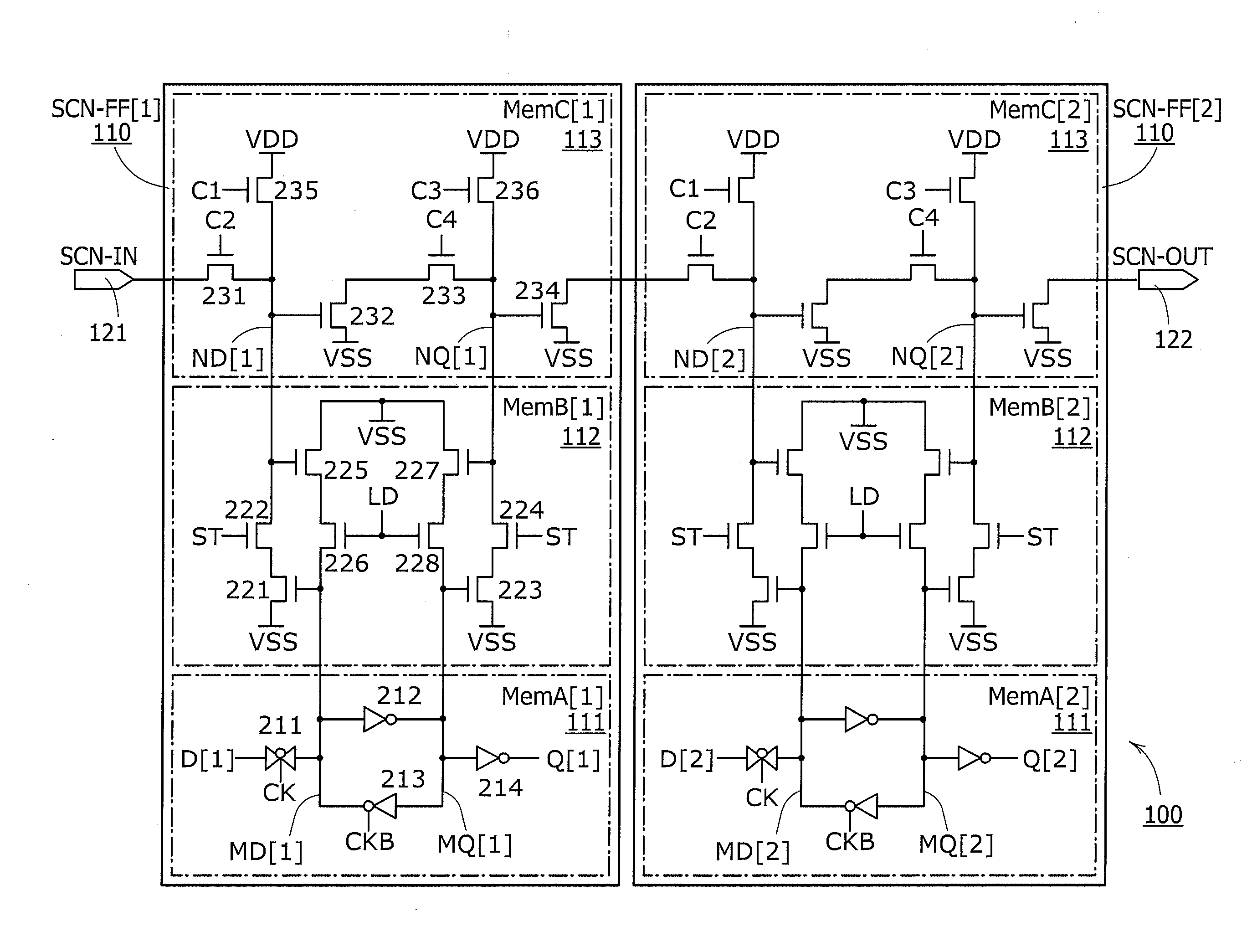
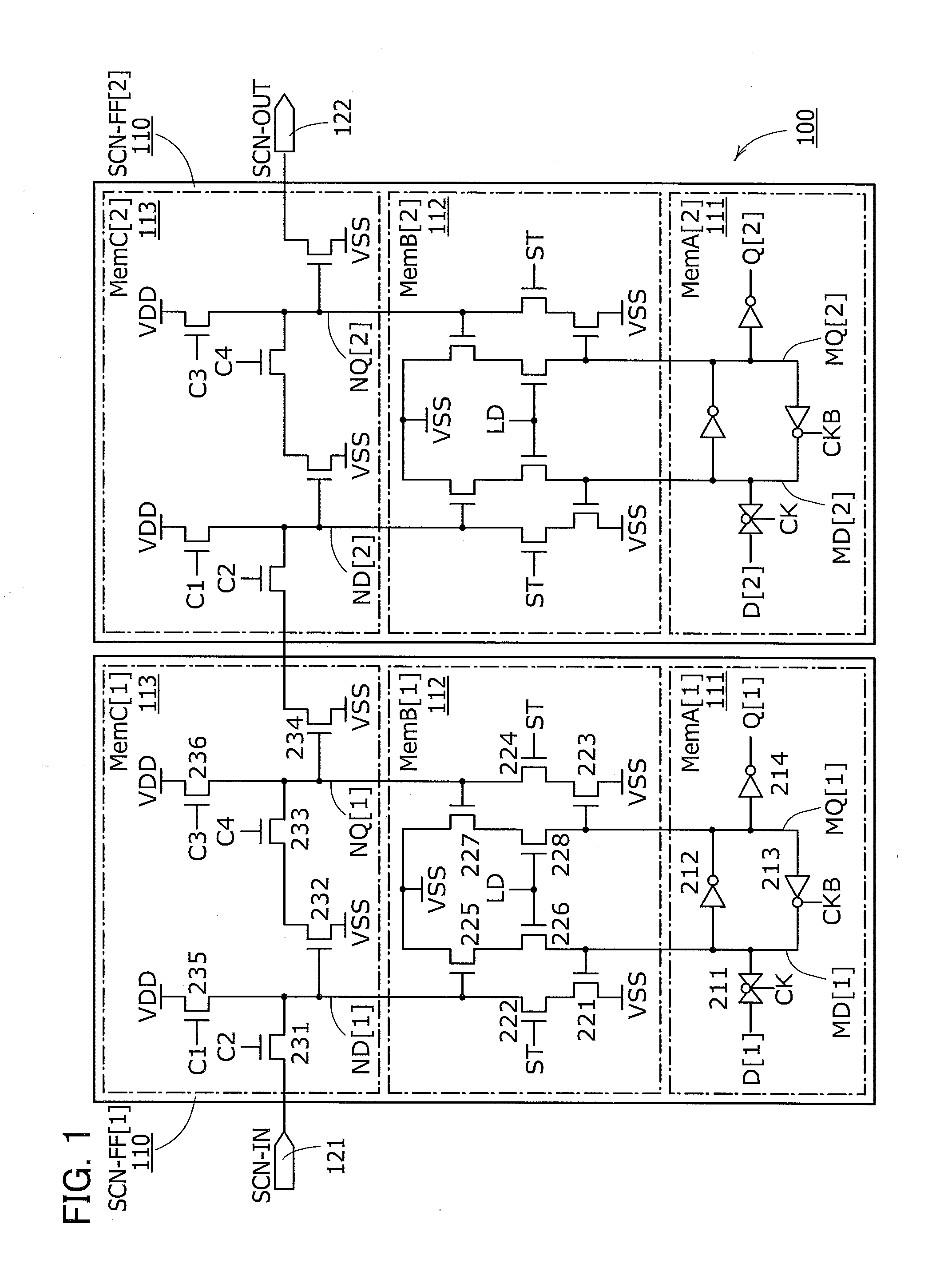
[0036]In this embodiment, a shift register which can be used for a scan test is described as an example of a semiconductor device. This embodiment will be described below with reference to FIG. 1, FIGS. 2A and 2B, FIG. 3, FIG. 4, and FIG. 5.
[0037]The shift register of this embodiment can be incorporated in a variety of integrated circuits such as a PLD, a CPU, and an MPU as a memory circuit and a verification circuit for a scan test.
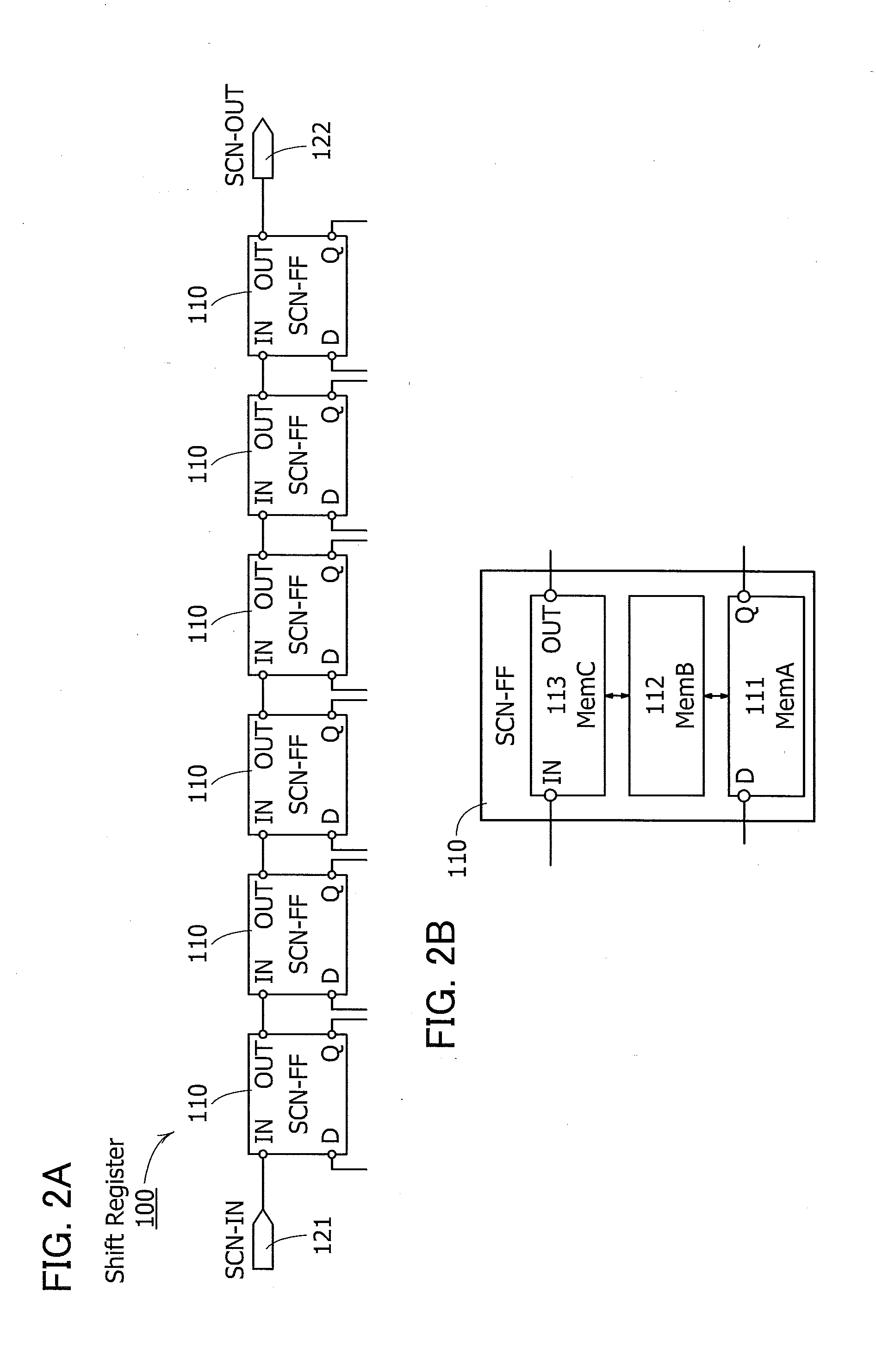
[0038]FIG. 2A is a block diagram illustrating a configuration example of a shift register (scan chain) for a scan test. FIG. 2B is a block diagram illustrating a configuration example of a scan flipflop included in the shift register. Further, FIG. 3 is a block diagram of an integrated circuit including the shift register in FIG. 2A.
[0039]A shift register 100 in FIG. 2A includes a plurality of scan flipflops 110 connected in a cascade. As shown in FIG. 2A, output terminals OUT of the scan flipflops 110 are connected to input terminals IN of the scan flip...
embodiment 2
[0112]The shift register 100 described in Embodiment 1 and functional circuits such as a combination circuit can be incorporated in one IC chip. In this embodiment, a structure example in which an integrated circuit capable of a scan test is used as one IC chip.
[0113]FIG. 6 illustrates an example of a cross-sectional structure of an integrated circuit. In FIG. 6, an OS transistor including a channel formation region in an oxide semiconductor layer and two transistors each including a channel formation region in a semiconductor substrate are illustrated as main elements included in the integrated circuit. Note that the cross-sectional view in FIG. 6 is not a cross-sectional view taken along a specific portion of the integrated circuit but a cross-sectional view for illustrating a layered structure of the integrated circuit.
[0114]A semiconductor substrate 500 can be, for example, an n-type or p-type single crystal silicon substrate, compound semiconductor substrate (e.g., a GaAs subst...
embodiment 3
[0177]In this embodiment, a structure and a manufacturing method of an oxide semiconductor transistor are described with reference to FIGS. 7A to 7C, FIGS. 8A to 8C, FIGS. 9A and 9B, FIGS. 10A to 10C, FIGS. 11A to 11D, and FIGS. 12A to 12D. The oxide semiconductor transistor in this embodiment can be manufactured, for example, as the OS transistor 560 of the integrated circuit in FIG. 6.
[0178]FIGS. 7A to 7C show a structure example of a top-gate OS transistor. FIG. 7A is a top view of an OS transistor 651, FIG. 7B is a cross-sectional view taken along line B1-B2 in FIG. 7A, and FIG. 7C is a cross-sectional view taken along line B3-B4 in FIG. 7A.
[0179]As illustrated in FIG. 7B, the OS transistor 651 includes a base insulating film 602 over a substrate 600, a multilayer film 606 over the base insulating film 602, a source electrode 616a, a drain electrode 616b, a gate insulating film 612, a gate electrode 604, and a protective insulating film 618.
[0180]The gate insulating film 612 is ...
PUM
 Abstract
Description
Claims
Application Information